Virtex-5 FPGA User Guide www.xilinx.com 355
UG190 (v5.0) June 19, 2009
Input Serial-to-Parallel Logic Resources (ISERDES)
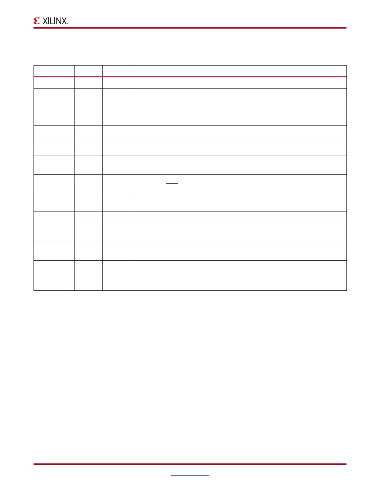
Table 8-1 lists the available ports in the ISERDES_NODELAY primitive.
ISERDES_NODELAY Ports
Registered Outputs - Q1 to Q6
The output ports Q1 to Q6 are the registered outputs of the ISERDES_NODELAY module.
One ISERDES_NODELAY block can support up to six bits (i.e., a 1:6 deserialization). Bit
widths greater than six (up to 10) can be supported. See “ISERDES Width Expansion.” The
first data bit received appears on the highest order Q output.
The bit ordering at the input of an OSERDES is the opposite of the bit ordering at the
output of an ISERDES_NODELAY block, as shown in Figure 8-3. For example, the least
significant bit A of the word FEDCBA is placed at the D1 input of an OSERDES, but the
same bit A emerges from the ISERDES_NODELAY block at the Q6 output. In other words,
D1 is the least significant input to the OSERDES, while Q6 is the least significant output of
the ISERDES_NODELAY block. When width expansion is used, D1 of the master
OSERDES is the least significant input, while Q4 of the slave ISERDES_NODELAY block is
the least significant output.
Table 8-1: ISERDES_NODELAY Port List and Definitions
Port Name Type Width Description
Q1 – Q6 Output 1 (each) Registered outputs. See “Registered Outputs - Q1 to Q6.”
SHIFTOUT1 Output 1 Carry out for data width expansion. Connect to SHIFTIN1 of slave IOB. See
“ISERDES Width Expansion.”
SHIFTOUT2 Output 1 Carry out for data width expansion. Connect to SHIFTIN2 of slave IOB. See
“ISERDES Width Expansion.”
BITSLIP Input 1 Invokes the Bitslip operation. See “Bitslip Operation - BITSLIP.”
CE1
CE2
Input 1 (each) Clock enable inputs. See “Clock Enable Inputs - CE1 and CE2.”
CLK Input 1 High-speed clock input. Clocks serial input data stream. See “High-Speed Clock
Input - CLK.”
CLKB Input 1 High-speed secondary clock input. Clocks serial input data stream. Always
connect this CLK
.
CLKDIV Input 1 Divided clock input. Clocks delay element, deserialized data, Bitslip submodule,
and CE unit. See “Divided Clock Input - CLKDIV.”
D Input 1 Serial input data from IOB. See “Serial Input Data from IOB - D.”
OCLK Input 1 High-speed clock input for memory applications. See “High-Speed Clock for
Strobe-Based Memory Interfaces - OCLK.”
SHIFTIN1 Input 1 Carry input for data width expansion. Connect to SHIFTOUT1 of master IOB. See
“ISERDES Width Expansion.”
SHIFTIN2 Input 1 Carry input for data width expansion. Connect to SHIFTOUT2 of master IOB. See
“ISERDES Width Expansion.”
RST Input 1 Active High reset. See “Reset Input - RST.”
 Loading...


