102 www.xilinx.com Virtex-5 FPGA User Guide
UG190 (v5.0) June 19, 2009
Chapter 3: Phase-Locked Loops (PLLs)
Counter Control
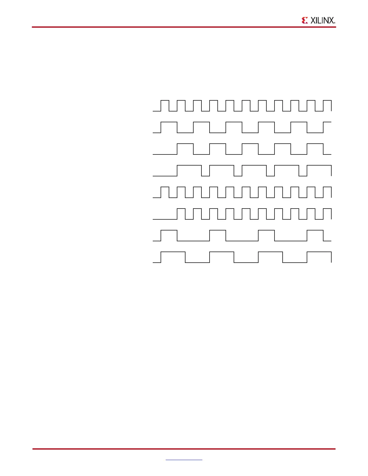
The PLL output counters provide a wide variety of synthesized clock using a combination
of DIVIDE, DUTY_CYCLE, and PHASE. Figure 3-6 illustrates how the counter settings
impact the counter output.
The top waveform represents either the output from the VCO in PLL mode.
X-Ref Target - Figure 3-6
Figure 3-6: Output Counter Clock Synthesis Examples
Counter Clock Input
(VCO)
DIVIDE = 2
DUTY_CYCLE = 0.5
PHASE = 0
DIVIDE = 2
DUTY_CYCLE = 0.5
PHASE = 180
DIVIDE = 2
DUTY_CYCLE = 0.75
PHASE = 180
DIVIDE = 1
DUTY_CYCLE = 0.5
PHASE = 0
DIVIDE = 1
DUTY_CYCLE = 0.5
PHASE = 360
DIVIDE = 3
DUTY_CYCLE = 0.33
PHASE = 0
DIVIDE = 3
DUTY_CYCLE = 0.5
PHASE = 0
UG190_3_06_041406
 Loading...


