158 www.xilinx.com Virtex-5 FPGA User Guide
UG190 (v5.0) June 19, 2009
Chapter 4: Block RAM
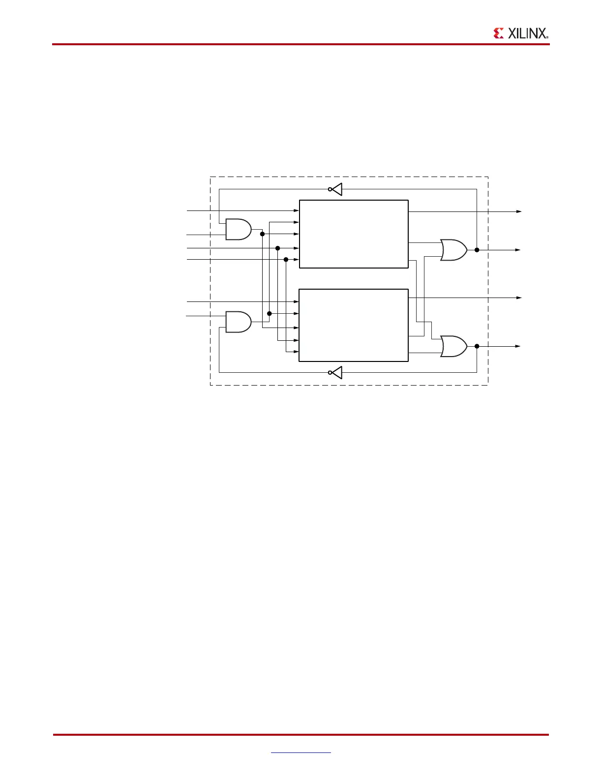
Connecting FIFOs in Parallel to Increase Width
As shown in Figure 4-27, the Virtex-5 FPGA FIFO36 can be connected to add width to the
design. CLB logic is used to implement the AND/OR gates. All the FIFO AFULL signals
must be ORed together to created the output AFULL signal and all the FIFO EMPTY
signals must be ORed together to created the output EMPTY signal. The maximum
frequency is limited by the logic gate feedback path.
Built-in Error Correction
Each simple dual-port block RAM can be configured as a single 512 x 64 RAM with built in
Hamming code error correction, using the extra eight bits in the 72-bit wide RAM. The
operation is transparent to the user.
Eight protection bits (ECCPARITY) are generated during each write operation and stored
with the 64-bit data into the memory. These ECCPARITY bits are used during each read
operation to correct any single-bit error, or to detect (but not correct) any double-bit error.
The ECCPARITY bits are written into the memory and output to the FPGA fabric at each
rising edge of the WRCLK. There are no optional output registers available on the
ECCPARITY output bits.
During each read operation, 72 bits of data (64 bits of data and an 8-bit parity) are read
from the memory and fed into the ECC decoder. The ECC decoder generates two status
outputs (SBITERR and DBITERR) that are used to indicate the three possible read results:
No error, single-bit error corrected, double-bit error detected. In the standard ECC mode,
the read operation does not correct the error in the memory array, it only presents corrected
data on DO. To improve F
MAX
, optional registers controlled by the DO_REG attribute are
available for data output (DO), SBITERR, and DBITERR.
This ECC configuration option is available with a 36K block RAM simple dual-port
primitive (RAMB36SDP) or a 36K FIFO primitive (FIFO36_72). A Virtex-4 FPGA ECC 18K
block RAM mapped for a Virtex-5 FPGA design will occupy the entire RAMB36 site.
FIFO36_72 supports standard ECC mode only.
X-Ref Target - Figure 4-27
Figure 4-27: Example: Connecting FIFOs in Parallel to Increase Width
RDCLK
WRCLK
DIN<71:0>
RDEN
WREN
RDCLK
WRCLK
DIN<71:0>
DOUT<71:0>
EMPTY
RDEN
WREN
AFULL
DOUT<71:0>
EMPTY
AFULL
DIN<71:0>
DIN<143:72>
DOUT<71:0>
DOUT<143:72>
RDEN
WREN
WRCLK
RDCLK
512 x 144 FIFO
FIFO #1
FIFO #2
AFULL
EMPTY
ug190_4_24_012706
 Loading...


