378 www.xilinx.com Virtex-5 FPGA User Guide
UG190 (v5.0) June 19, 2009
Chapter 8: Advanced SelectIO Logic Resources
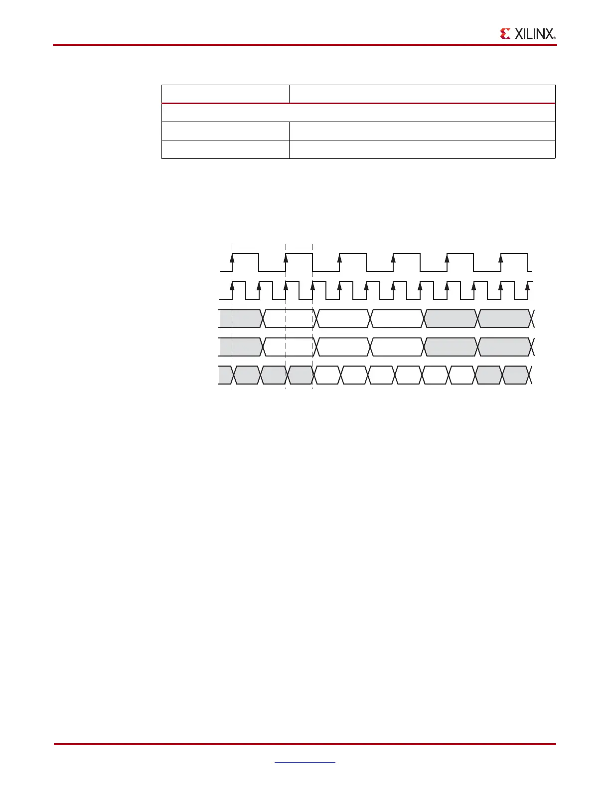
Timing Characteristics of 2:1 SDR Serialization
In Figure 8-17, the timing of a 2:1 SDR data serialization is illustrated.
Clock Event 1
On the rising edge of CLKDIV, the word AB is driven from the FPGA logic to the D1 and
D2 inputs of the OSERDES (after some propagation delay).
Clock Event 2
On the rising edge of CLKDIV, the word AB is sampled into the OSERDES from the D1 and
D2 inputs.
Clock Event 3
The data bit A appears at OQ one CLK cycle after AB is sampled into the OSERDES. This
latency is consistent with the Table 8-10 listing of a 2:1 SDR mode OSERDES latency of one
CLK cycle.
Combinatorial
T
OSCO_OQ
Asynchronous Reset to OQ
T
OSCO_TQ
Asynchronous Reset to TQ
Table 8-11: OSERDES Switching Characteristics (Continued)
Symbol Description
X-Ref Target - Figure 8-17
Figure 8-17: OSERDES Data Flow and Latency in 2:1 SDR Mode
UG190_8_17_100307
D2
BD
CLKDIV
CLK
ABCDEF
OQ
D1
AC
F
E
Clock
Event 1
Clock
Event 2
Clock
Event 3
 Loading...


