170 www.xilinx.com Virtex-5 FPGA User Guide
UG190 (v5.0) June 19, 2009
Chapter 4: Block RAM
Creating a Deliberate Error in a 72-bit Word
To deliberately create an error in a 72-bit word, configure the ECC decode-only mode and
create a 72-bit word with one or two bit errors. Write the word into the block RAM.
Reading the 72-bit word automatically corrects the single-bit error and asserts the
SBITERR error flag or it detects the double-bit error and asserts the DBITERR error flag.
Creating Eight Parity Bits for a 64-bit Word
Using logic external to the block RAM (a large number of XOR circuits), eight parity bits
can be created for a 64-bit word. However, using ECC encoder-only mode, the eight parity
bits can be automatically created without additional logic by writing any 64-bit word into
a separate block RAM. The encoded 8-bit ECC parity data is immediately available, or the
complete 72-bit word can be read out.
Inserting a Single or Double Bit Error into a 72-bit Word
By reading a 72-bit word and selectively modifying one or two bits, then writing all 72 bits
into the block RAM under test in ECC decode-only mode, a single or double bit error can
be inserted.
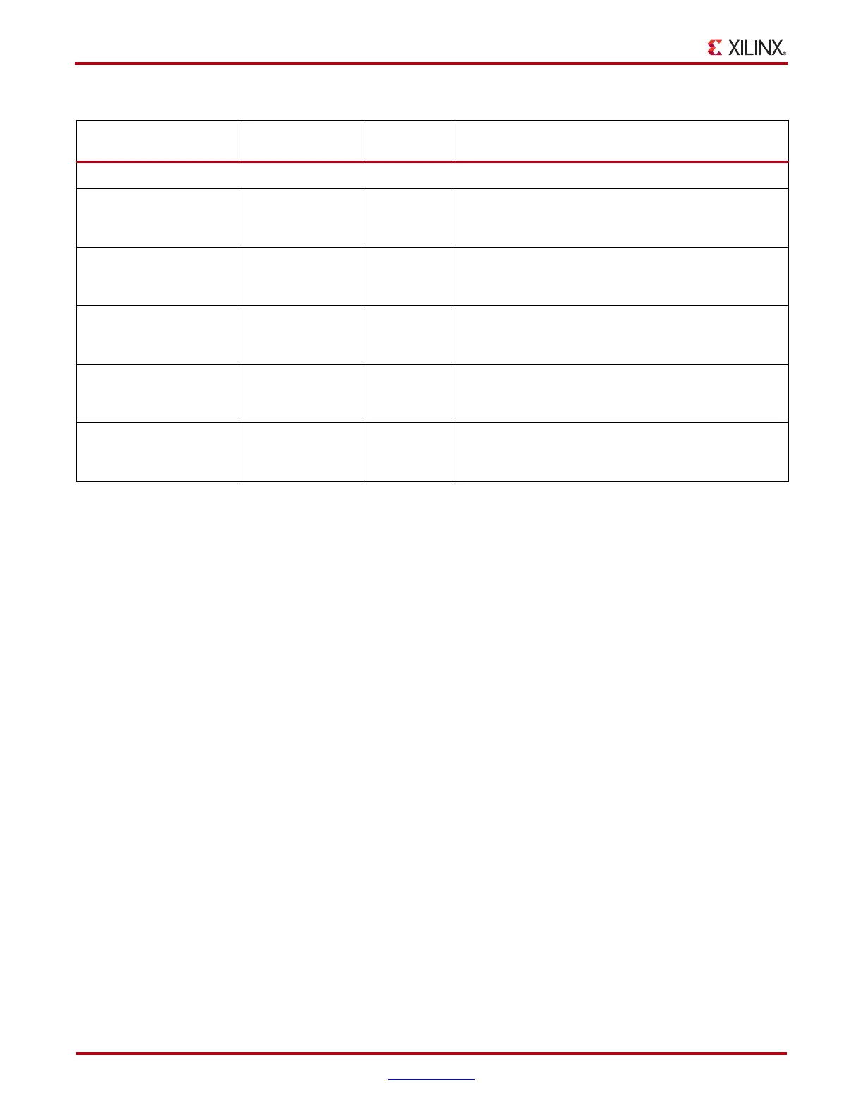
Clock to ECC Delays
T
RCKO_ECC_PARITY
(encode-only mode)
(3)
Clock to ECC
Parity Output
ECCPARITY Time after WRCLK that the ECC parity signals are
stable at the ECCPARITY outputs of the block RAM (in
encode-only mode).
T
RCKO_ECC_SBITERR
(3)
Clock to ECC
Single-Bit-Error
Output
SBITERR Time after RDCLK that the single-bit-error signal is
stable at the SBITERR output of the block RAM
(without output register).
T
RCKO_ECCR_SBITERR
(4)
Clock to ECC
Single-Bit-Error
Output
SBITERR Time after RDCLK that the single-bit-error signal is
stable at the SBITERR output of the block RAM (with
output register).
T
RCKO_ECC_DBITERR
(3)
Clock to ECC
Double-Bit-Error
Output
DBITERR Time after RDCLK that the double-bit-error signal is
stable at the DBITERR output of the block RAM
(without output register).
T
RCKO_ECCR_DBITERR
(4)
Clock to ECC
Double-Bit-Error
Output
DBITERR Time after RDCLK that the double-bit-error signal is
stable at the DBITERR output of the block RAM (with
output register).
Notes:
1. T
RDCK_DI_ECC
/T
RCKD_DI_ECC
include the parity input T
RDCK_DIP_ECC
/T
RCKD_DIP_ECC
.
2. T
RCKO_DO
includes parity output (T
RCKO_DOP
).
3. T
RCKO_ECC_PARITY
, T
RCKO_ECC_SBITERR
, and T
RCKO_ECC_DBITERR
are combined into the T
RCKO_ECC
parameter in the Virtex-5 FPGA
Data Sheet.
4. T
RCKO_ECC_SBITERR
and T
RCKO_ECC_DBITERR
are combined into the T
RCKO_ECCR
parameter in the Virtex-5 FPGA Data Sheet.
Table 4-25: Block RAM ECC Mode Timing Parameters (Continued)
Parameter Function
Control
Signal
Description
 Loading...


