Virtex-5 FPGA User Guide www.xilinx.com 347
UG190 (v5.0) June 19, 2009
OLOGIC Resources
Clock Forwarding
Output DDR can forward a copy of the clock to the output. This is useful for propagating
a clock and DDR data with identical delays, and for multiple clock generation, where every
clock load has a unique clock driver. This is accomplished by tying the D1 input of the
ODDR primitive High, and the D2 input Low. Xilinx recommends using this scheme to
forward clocks from the FPGA fabric to the output pins.
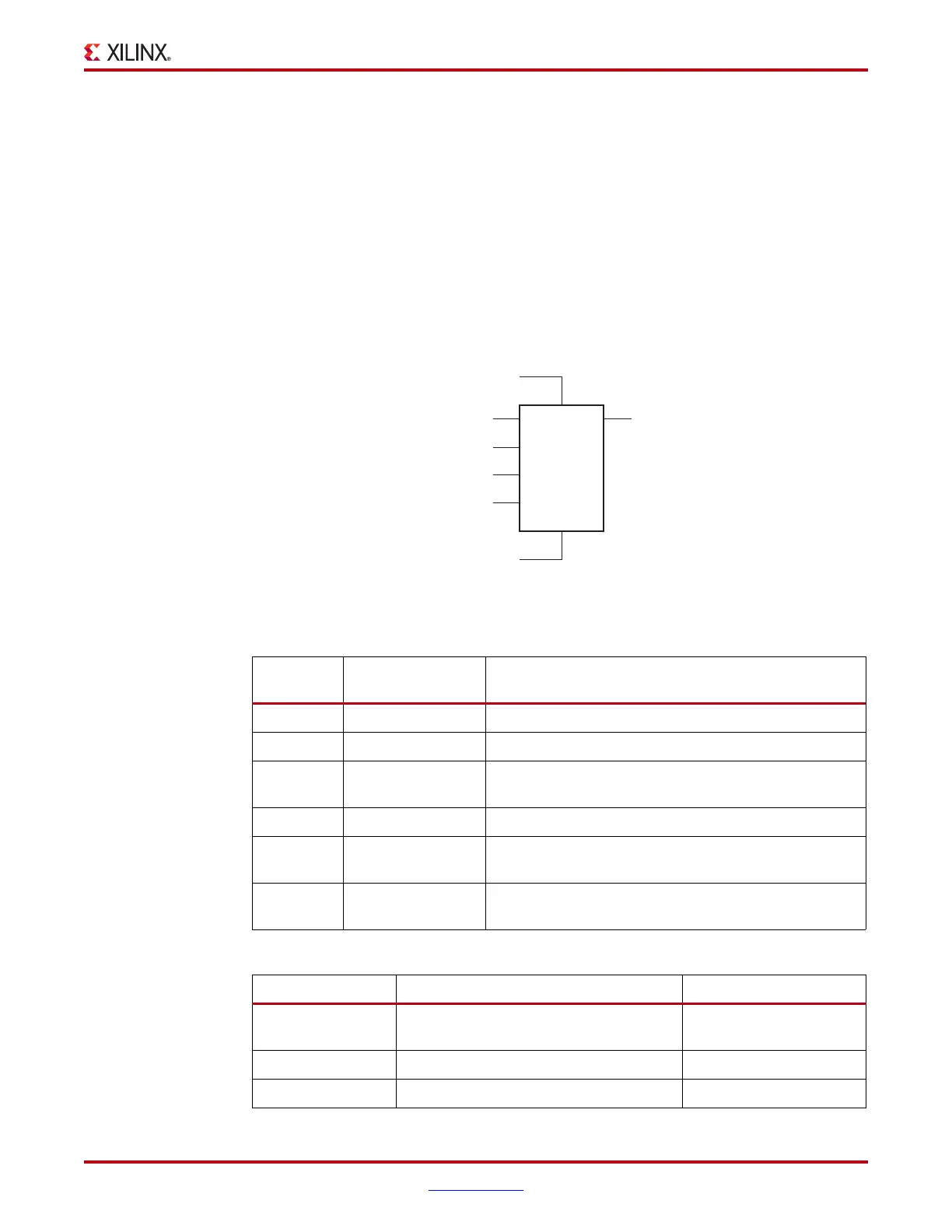
Output DDR Primitive (ODDR)
Figure 7-25 shows the ODDR primitive block diagram. Table 7-13 lists the ODDR port
signals. Table 7-14 describes the various attributes available and default values for the
ODDR primitive.
X-Ref Target - Figure 7-25
Figure 7-25: ODDR Primitive Block Diagram
Table 7-13: ODDR Port Signals
Port
Name
Function Description
Q Data output (DDR) ODDR register output.
C Clock input port The CLK pin represents the clock input pin.
CE Clock enable port CE represents the clock enable pin. When asserted Low,
this port disables the output clock on port Q.
D1 and D2 Data inputs ODDR register inputs.
R Reset Synchronous/Asynchronous reset pin. Reset is asserted
High.
S Set Synchronous/Asynchronous set pin. Set is asserted
High.
Table 7-14: ODDR Attributes
Attribute Name Description Possible Values
DDR_CLK_EDGE Sets the ODDR mode of operation with
respect to clock edge
OPPOSITE_EDGE
(default), SAME_EDGE
INIT Sets the initial value for Q port 0 (default), 1
SRTYPE Set/Reset type with respect to clock (C) ASYNC, SYNC (default)
ug190_7_20_012207
C
CE
D1
S
R
Q
D2
ODDR
 Loading...


