Virtex-5 FPGA User Guide www.xilinx.com 273
UG190 (v5.0) June 19, 2009
Specific Guidelines for I/O Supported Standards
Table 6-26 lists the HSTL Class IV (1.8V) DC voltage specifications.
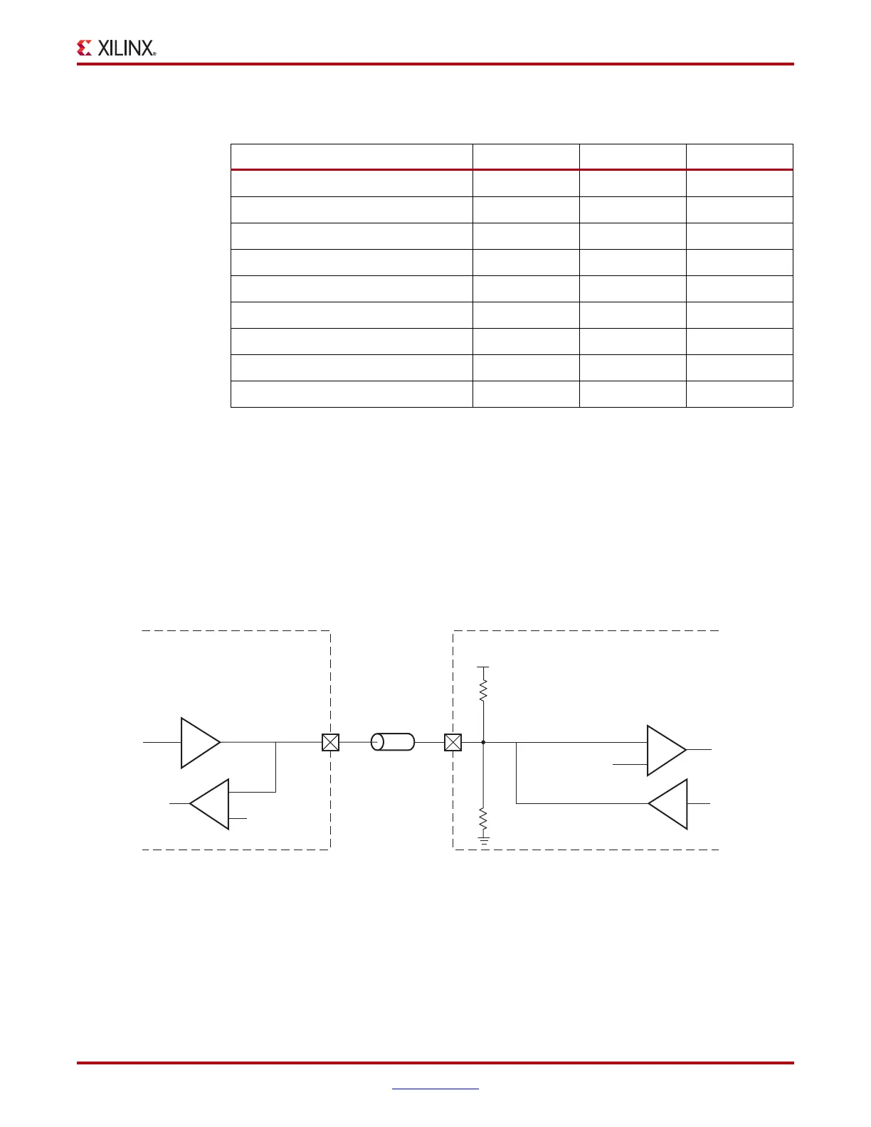
HSTL_II_T_DCI_18 (1.8V) Split-Thevenin Termination
Figure 6-65 shows a sample circuit illustrating a valid termination technique for
HSTL_II_T_DCI_18 (1.8V) with on-chip split-thevenin termination. In this bidirectional
case, when 3-stated, the termination is invoked on the receiver and not on the driver.
Table 6-26: HSTL Class IV (1.8V) DC Voltage Specifications
Min Typ Max
V
CCO
1.7 1.8 1.9
V
REF
(2)
– 1.1 –
V
TT
– V
CCO
–
V
IH
V
REF
+0.1 – –
V
IL
––V
REF
–0.1
V
OH
V
CCO
–0.4 – –
V
OL
– – 0.4
I
OH
at V
OH
(mA)
(1)
–8 – –
I
OL
at V
OL
(mA)
(1)
48 – –
Notes:
1. V
OL
and V
OH
for lower drive currents are sample tested.
2. Per EIA/JESD8-6, “The value of V
REF
is to be selected by the user to provide optimum noise margin in
the use conditions specified by the user.”
X-Ref Target - Figure 6-65
Figure 6-65: HSTL_II_T_DCI_18 Split-Thevenin Termination
ug190_6_91_041206
Z
0
IOB
IOB
HSTL_II_T_DCI_18
HSTL_II_T_DCI_18
V
CCO
= 1.8V
2R
VRP
= 2Z
0
= 100Ω
2R
VRN
= 2Z
0
= 100Ω
V
REF
= 0.9V
+
–
DCI
V
REF
= 0.9V
Not 3-stated 3-stated
 Loading...


