376 www.xilinx.com Virtex-5 FPGA User Guide
UG190 (v5.0) June 19, 2009
Chapter 8: Advanced SelectIO Logic Resources
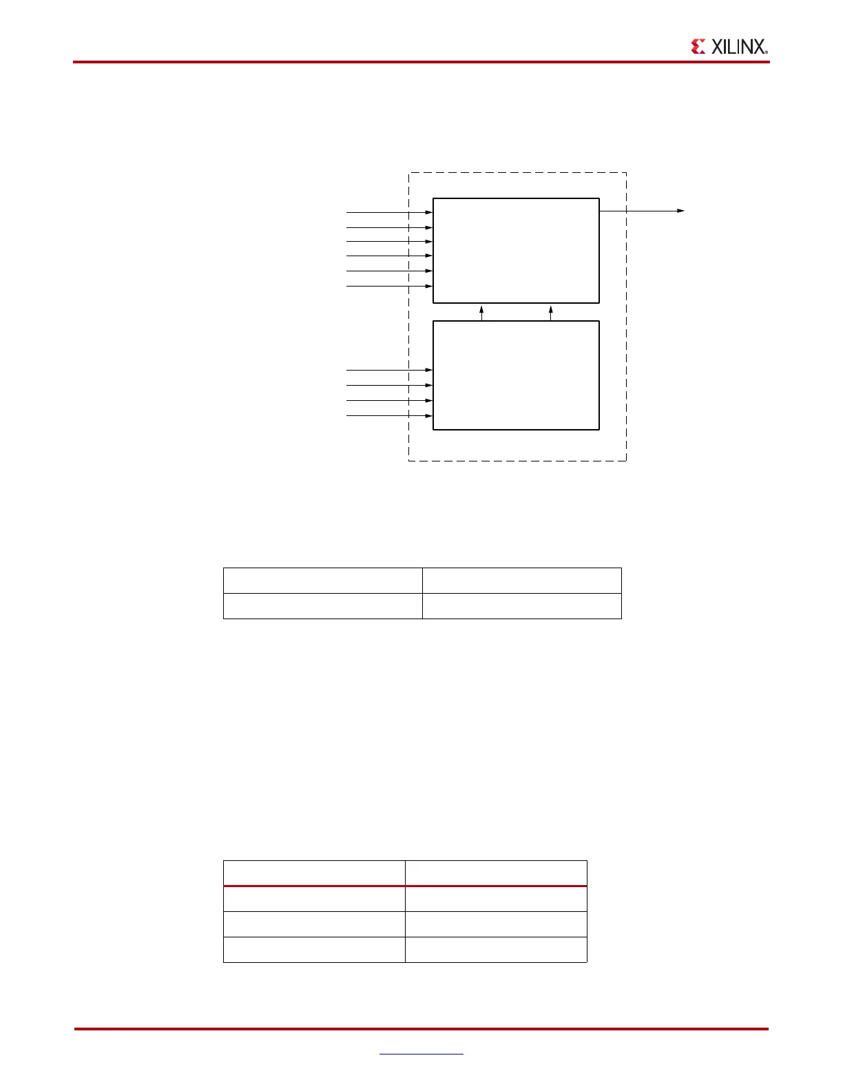
Figure 8-16 illustrates a block diagram of a 10:1 DDR parallel-to-serial converter using the
master and slave OSERDES modules. Ports Q3-Q6 are used for the last four bits of the
parallel interface on the slave OSERDES (LSB to MSB).
Table 8-8 lists the data width availability for SDR and DDR mode.
Guidelines for Expanding the Parallel-to-Serial Converter Bit Width
1. Both the OSERDES modules must be adjacent master and slave pairs.
2. Set the SERDES_MODE attribute for the master OSERDES to MASTER and the slave
OSERDES to SLAVE. See “SERDES_MODE Attribute.”
3. The user must connect the SHIFTIN ports of the MASTER to the SHIFTOUT ports of
the SLAVE.
4. The SLAVE only uses the ports D3 to D6 as an input.
5. DATA_WIDTH for Master and Slave are equal. See “DATA_WIDTH Attribute.”
The slave inputs used for data widths requiring width expansion are listed in Table 8-9.
X-Ref Target - Figure 8-16
Figure 8-16: Block Diagram of OSERDES Width Expansion
Table 8-8: OSERDES SDR/DDR Data Width Availability
SDR Data Widths 2, 3, 4, 5, 6, 7, 8
DDR Data Widths 4, 6, 8, 10
OQ
Data Inputs[0:5]
Data Inputs[6:9]
OSERDES
(Slave)
SERDES_MODE=SLAVE
OQ
OSERDES
(Master)
SERDES_MODE = MASTER
D1
D2
D3
D4
D5
D6
D1
D2
D3
D4
D5
D6
SHIFTIN1 SHIFTIN2
SHIFTOUT1 SHIFTOUT2
Data Out
ug190_8_16_100307
Table 8-9: Slave Inputs Used for Data Width Expansion
Data Width Slave Inputs Used
7D3
8D3–D4
10 D3–D6
 Loading...


