86 www.xilinx.com Virtex-5 FPGA User Guide
UG190 (v5.0) June 19, 2009
Chapter 2: Clock Management Technology
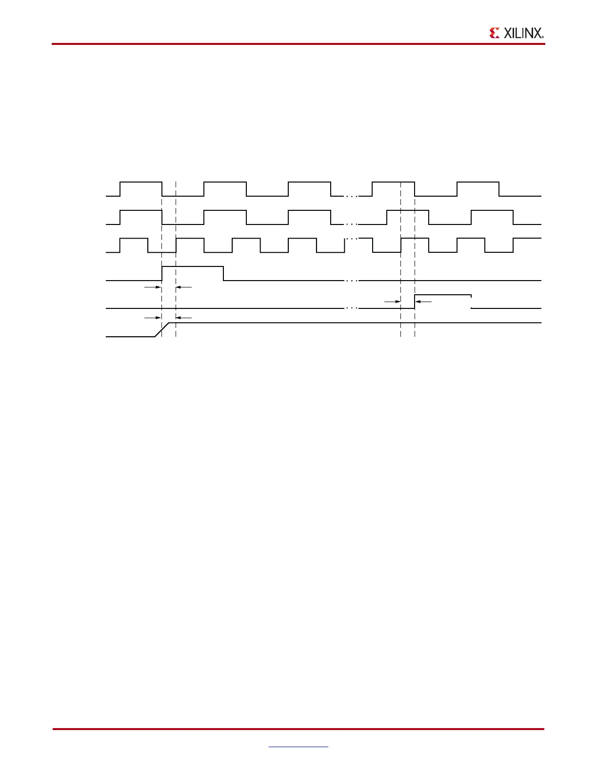
Variable-Phase Shifting
In Figure 2-19, the CLK0 output is phase-shifted using the dynamic phase-shift
adjustments in the synchronous user interface. The PSDONE signal is asserted for one
cycle when the DCM completes one phase adjustment. After PSDONE is deasserted, PSEN
can be asserted again, allowing an additional phase shift to occur.
As shown in Figure 2-19, all the variable-phase shift control and status signals are
synchronous to the rising edge of PSCLK.
• Clock Event 1
At T
DMCCK_PSEN
, before clock event 1, PSEN is asserted. PSEN must be active for
exactly one clock period; otherwise, a single increment/decrement of phase shift is not
guaranteed. Also, the PSINCDEC value at T
DMCCK_PSINCDEC
, before clock event 1,
determines whether it is an increment (logic High) or a decrement (logic Low).
• Clock Event 2
At T
DMCKO_PSDONE
, after clock event 2, PSDONE is asserted to indicate one increment
or decrement of the DCM outputs. PSDONE is High for exactly one clock period when
the phase shift is complete. The time required for a complete phase shift varies. As a
result, PSDONE must be monitored for phase-shift status.
X-Ref Target - Figure 2-19
Figure 2-19: Phase Shift Example: Variable
CLKIN
CLK0
PSCLK
PSEN
PSDONE
PSINCDEC
1
D.C. D.C.
2
T
DMCCK_PSEN
T
DMCKO_PSDONE
T
DMCCK_PSINCDEC
ug190_2_20_0042406
 Loading...


