226 www.xilinx.com Virtex-5 FPGA User Guide
UG190 (v5.0) June 19, 2009
Chapter 6: SelectIO Resources
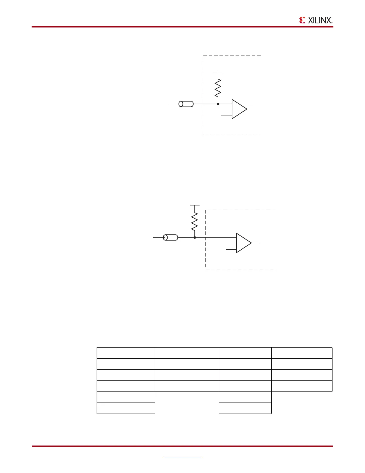
Figure 6-9 illustrates DCI single termination inside a Virtex-5 device.
Input Termination to V
CCO
/2 (Split Termination)
Some I/O standards (e.g., HSTL Class I and II) require an input termination voltage of
V
CCO
/2 (see Figure 6-10).
This is equivalent to having a split termination composed of two resistors. One terminates
to V
CCO
, the other to ground. The resistor values are 2R. DCI provides termination to
V
CCO
/2 using split termination. The termination resistance is set by the external reference
resistors, i.e., the resistors to V
CCO
and ground are each twice the reference resistor value.
Both HSTL and SSTL standards need 50 Ω external reference resistors. The DCI input
standards supporting split termination are shown in Table 6-1.
X-Ref Target - Figure 6-9
Figure 6-9: Input Termination Using DCI Single Termination
R
UG190_6_07_021206
V
CCO
V
REF
IOB
Z
0
Virtex-5 DCI
X-Ref Target - Figure 6-10
Figure 6-10: Input Termination to V
CCO
/2 without DCI
Table 6-1: DCI Input Standards Supporting Split Termination
HSTL_I_DCI DIFF_HSTL_I_DCI SSTL2_I_DCI DIFF_SSTL2_I_DCI
HSTL_I_DCI_18 DIFF_HSTL_I_DCI_18 SSTL2_II_DCI DIFF_SSTL2_II_DCI
HSTL_II_DCI DIFF_HSTL_II_DCI SSTL18_I_DCI DIFF_SSTL18_I_DCI
HSTL_II_DCI_18 DIFF_HSTL_II_DCI_18 SSTL18_II_DCI DIFF_SSTL18_II_DCI
HSTL_II_T_DCI SSTL2_II_T_DCI
HSTL_II_T_DCI_18 SSTL18_II_T_DCI
R
UG190_c6_08_022609
V
CCO
/2
V
REF
IOB
Z
0
Virtex-5 FPGA
 Loading...


