128 www.xilinx.com Virtex-5 FPGA User Guide
UG190 (v5.0) June 19, 2009
Chapter 4: Block RAM
Block RAM Address Mapping
Each port accesses the same set of 18,432 or 36,864 memory cells using an addressing
scheme dependent on whether it is a RAMB18 or RAMB36. The physical RAM locations
addressed for a particular width are determined using the following formula (of interest
only when the two ports use different aspect ratios):
END=((ADDR+1)
× Width) -1
START = ADDR
× Width
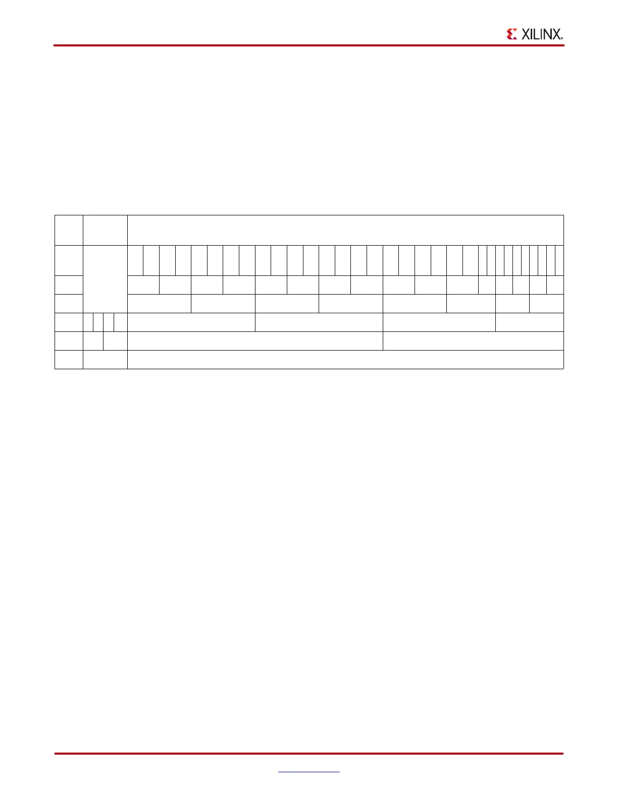
Table 4-8 shows low-order address mapping for each port width.
Block RAM Attributes
All attribute code examples are discussed in the “Block RAM Initialization in VHDL or
Verilog Code” section. Further information on using these attributes is available in the
“Additional RAMB18 and RAMB36 Primitive Design Considerations” section.
Content Initialization - INIT_xx
INIT_xx attributes define the initial memory contents. By default, block RAM memory is
initialized with all zeros during the device configuration sequence. The 64 initialization
attributes from INIT_00 through INIT_3F for the RAMB18, and the 128 initialization
attributes from INIT_00 through INIT_7F for the RAMB36 represent the regular memory
contents. Each INIT_xx is a 64-digit hex-encoded bit vector. The memory contents can be
partially initialized and are automatically completed with zeros.
The following formula is used for determining the bit positions for each INIT_xx attribute.
Given yy = conversion hex-encoded to decimal (xx), INIT_xx corresponds to the memory
cells as follows:
• from [(yy + 1) × 256] – 1
• to (yy) × 256
For example, for the attribute INIT_1F, the conversion is as follows:
• yy = conversion hex-encoded to decimal (xx) “1F” = 31
• from [(31+1) × 256] – 1 = 8191
• to 31 × 256 = 7936
More examples are given in Table 4-9.
Table 4-8: Port Address Mapping
Port
Width
Parity
Locations
Data Locations
1N.A.3
1
3
0
2
9
2
8
2
7
2
6
2
5
2
4
2
3
2
2
2
1
2
0
1
9
1
8
1
7
1
6
1
5
1
4
1
3
1
2
11 1
0
9876543210
2 1514131211109876543210
4 76543210
8 + 1 3 2 1 0 3 2 1 0
16 + 2 1 0 1 0
32 + 4 0 0
 Loading...


