248 www.xilinx.com Virtex-5 FPGA User Guide
UG190 (v5.0) June 19, 2009
Chapter 6: SelectIO Resources
GTL (Gunning Transceiver Logic)
The Gunning Transceiver Logic (GTL) standard is a high-speed bus standard (JESD8.3)
invented by Xerox. Xilinx has implemented the terminated variation for this standard. This
standard requires a differential amplifier input buffer and an open-drain output buffer.
The negative terminal of the differential input buffer is referenced to the V
REF
pin.
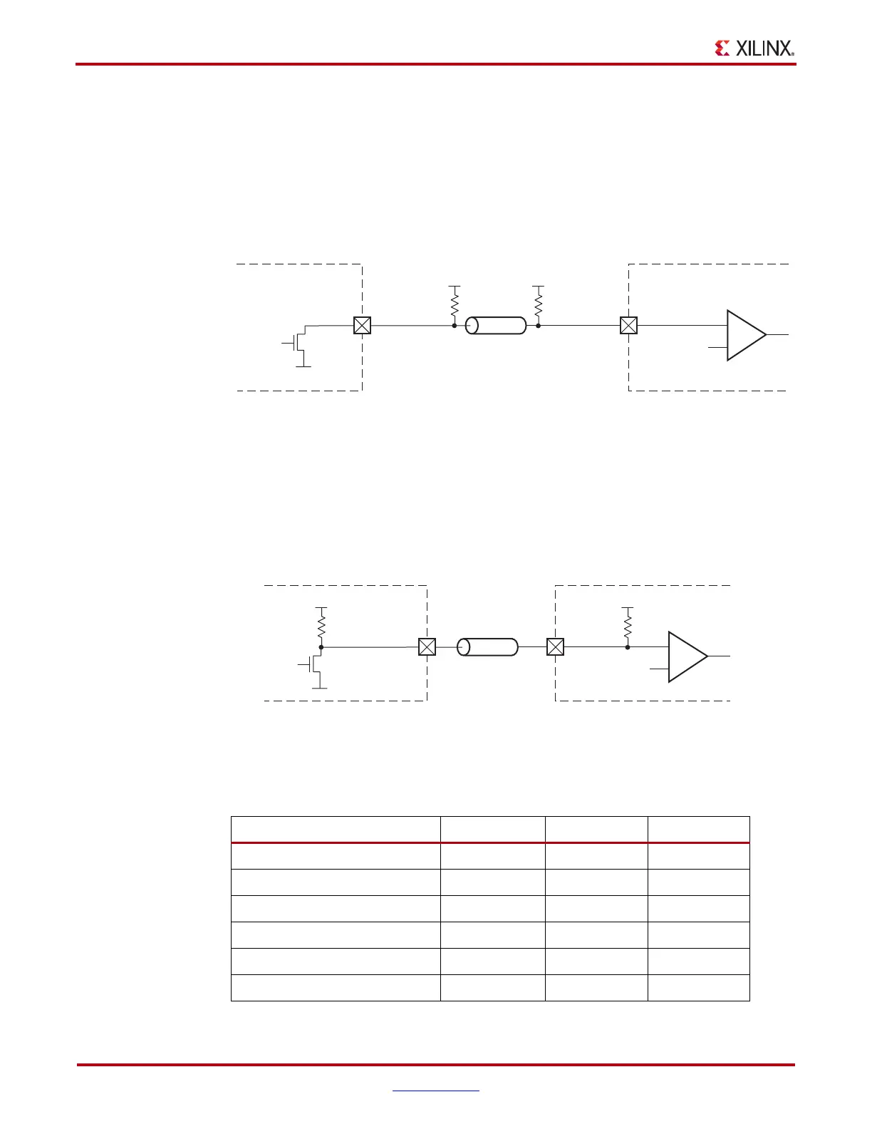
A sample circuit illustrating a valid termination technique for GTL with external parallel
termination and unconnected V
CCO
is shown in Figure 6-36.
GTL_DCI Usage
GTL does not require a V
CCO
voltage. However, for GTL_DCI, V
CCO
must be connected to
1.2V. GTL_DCI provides single termination to V
CCO
for inputs or outputs.
A sample circuit illustrating a valid termination technique for GTL_DCI with internal
parallel driver and receiver termination is shown in Figure 6-37.
Table 6-13 lists the GTL DC voltage specifications.
X-Ref Target - Figure 6-36
Figure 6-36: GTL with External Parallel Termination and Unconnected V
CCO
V
TT
= 1.2V
R
P
= Z
0
= 50Ω R
P
= Z
0
= 50Ω
V
CCO
= Unconnected
V
TT
= 1.2V
Z
0
= 50
IOB
IOB
ug190_6_34_022806
V
REF
= 0.8V
+
–
X-Ref Target - Figure 6-37
Figure 6-37: GTL_DCI with Internal Parallel Driver and Receiver Termination
Table 6-13: GTL DC Voltage Specifications
Parameter Min Typ Max
V
CCO
–N/A-
V
REF
= N × V
TT
(1)
0.74 0.8 0.86
V
TT
1.14 1.2 1.26
V
IH
= V
REF
+ 0.05 0.79 0.83 –
V
IL
= V
REF
– 0.05 – 0.77 0.81
V
OH
–––
V
CCO
= 1.2V
V
CCO
= 1.2V
Z
0
= 50
IOB
IOB
ug190_6_35_030206
V
REF
= 0.8V
+
–
R
VRP
= Z
0
= 50Ω
R
VRP
= Z
0
= 50Ω
 Loading...


