Virtex-5 FPGA User Guide www.xilinx.com 61
UG190 (v5.0) June 19, 2009
DCM Attributes
FACTORY_JF Attribute
The Factory_JF attribute affects the DCMs jitter filter characteristics. This attribute controls
the DCM tap update rate. The default value is 0xF0F0 corresponding to
DLL_FREQUENCY_MODE = LOW and DLL_FREQUENCY_MODE = HIGH.
PHASE_SHIFT Attribute
The PHASE_SHIFT attribute determines the amount of phase shift applied to the DCM
outputs. This attribute can be used in both fixed or variable phase-shift mode. If used with
variable mode, the attribute sets the starting phase shift. When
CLKOUT_PHASE_SHIFT = VARIABLE_POSITIVE, the PHASE_SHIFT value range is 0 to
255. When CLKOUT_PHASE_SHIFT = VARIABLE_CENTER or FIXED, the
PHASE_SHIFT value range is –255 to 255. When CLKOUT_PHASE_SHIFT = DIRECT, the
PHASE_SHIFT value range is 0 to 1023. The default value is 0.
Refer to the Phase Shifting section for information on the phase-shifting operation and its
relationship with the CLKOUT_PHASE_SHIFT and PHASE_SHIFT attributes.
STARTUP_WAIT Attribute
The STARTUP_WAIT attribute determines whether the DCM waits in one of the startup
cycles for the DCM to lock. The possible values for this attribute are TRUE and FALSE. The
default value is FALSE. When STARTUP_WAIT is set to TRUE, and the LCK_cycle BitGen
option is used, then the configuration startup sequence waits in the startup cycle specified
by LCK_cycle until the DCM is locked.
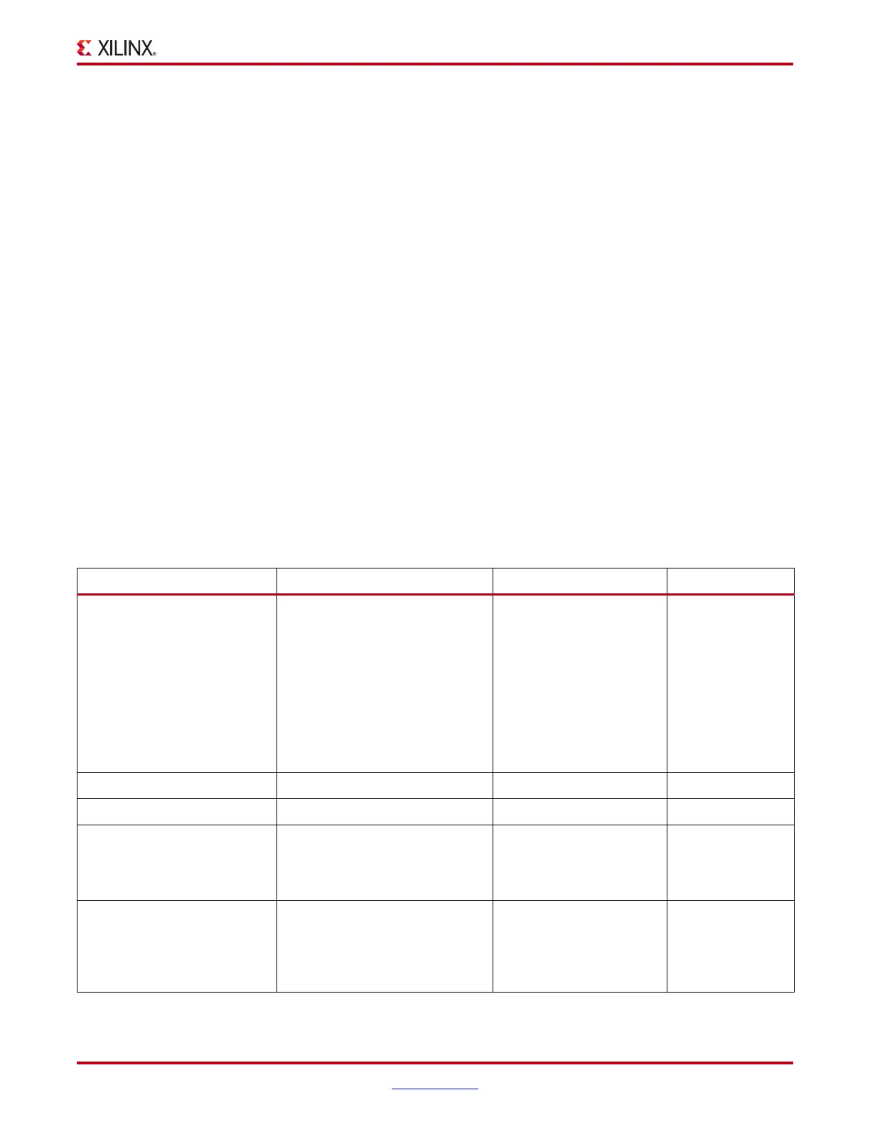
Table 2-6: DCM Attributes
DCM Attribute Name Description Values Default Value
CLKDV_DIVIDE This attribute controls CLKDV such
that the source clock is divided by
N.
This feature provides automatic
duty cycle correction such that the
CLKDV output pin has a 50/50 duty
cycle always in low-frequency
mode, as well as for all integer
values of the division factor N in
high-frequency mode.
Real:
1.5, 2.0, 2.5, 3.0, 3.5, 4.0, 4.5,
5.0, 5.5, 6.0, 6.5, 7.0, 7.5, 8, 9,
10, 11, 12, 13, 14, 15, 16
2.0
CLKFX_DIVIDE Integer: 1 to 32 1
CLKFX_MULTIPLY Integer: 2 to 32 4
CLKIN_PERIOD This specifies the source clock
period to help DCM adjust for
optimum CLKFX/CLKFX180
outputs.
Real in ns 0.0
CLKIN_DIVIDE_BY_2 This attribute allows for the input
clock frequency to be divided in half
when such a reduction is necessary
to meet the DCM input clock
frequency requirements.
Boolean: FALSE or TRUE FALSE
 Loading...


