246 www.xilinx.com Virtex-5 FPGA User Guide
UG190 (v5.0) June 19, 2009
Chapter 6: SelectIO Resources
HSLVDCI (High-Speed Low Voltage Digitally Controlled Impedance)
The HSLVDCI standard is intended for bidirectional use. The driver is identical to LVDCI,
while the input is identical to HSTL and SSTL. By using a V
REF
-referenced input,
HSLVDCI allows greater input sensitivity at the receiver than when using a single-ended
LVCMOS-type receiver.
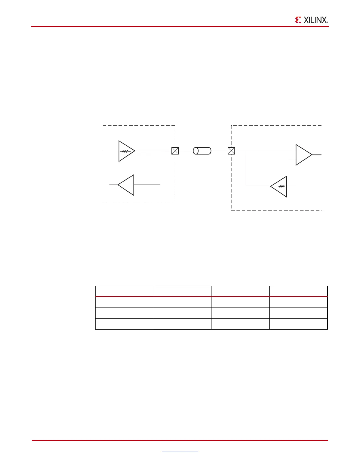
A sample circuit illustrating bidirectional termination techniques for an HSLVDCI
controlled impedance driver is shown in Figure 6-35. The DCI I/O standards supporting a
controlled impedance driver with a V
REF
referenced input are: HSLVDCI_15,
HSLVDCI_18, HSLVDCI_25, and HSLVDCI_33.
For output DC voltage specifications, refer to the LVDCI V
OH
and V
OL
entries in Table 6-9
“LVCMOS, LVDCI, and LVDCI_DV2 DC Voltage Specifications at Various Voltage
References.” Table 6-10 lists the input DC voltage specifications when using HSLVDCI.
Valid values of V
CCO
are 1.5V, 1.8V, 2.5V, and 3.3V. Select V
REF
to provide the optimum
noise margin in specific use conditions.
X-Ref Target - Figure 6-35
Figure 6-35: HSLVDCI Controlled Impedance Driver with Bidirectional Termination
Table 6-10: HSLVDCI Input DC Voltage Specifications
Standard Min Typ Max
V
REF
–V
CCO
/2 –
V
IH
V
REF
+0.1 – –
V
IL
––V
REF
–0.1
Z
0
IOB
HSLVDCI
ug190_6_33_022806
R
0
= R
VRN
= R
VRP
= Z
0
R
0
= R
VRN
= R
VRP
= Z
0
HSLVDCI
IOB
V
REF
= V
CCO
/2
+
–
 Loading...


