Virtex-5 FPGA User Guide www.xilinx.com 245
UG190 (v5.0) June 19, 2009
Specific Guidelines for I/O Supported Standards
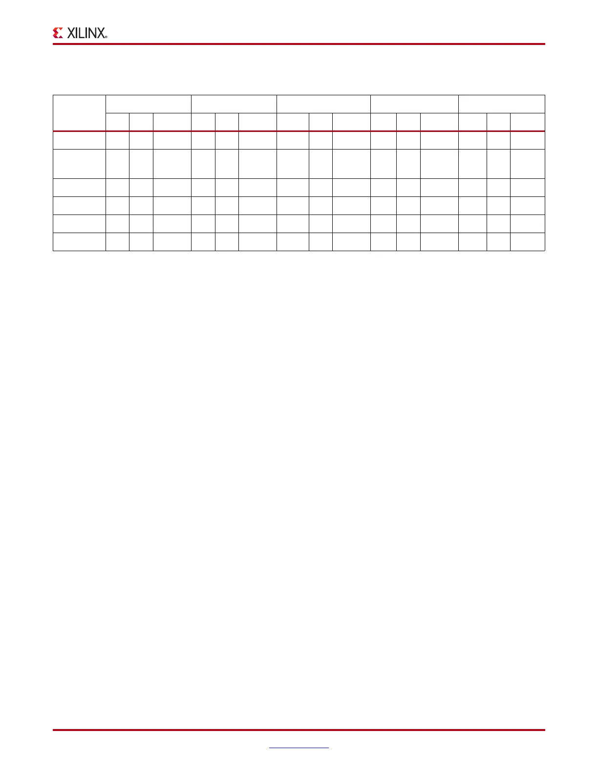
Table 6-9: LVCMOS, LVDCI, and LVDCI_DV2 DC Voltage Specifications
at Various Voltage References
Standard
+3.3V +2.5V +1.8V +1.5V +1.2V
(2)
Min Typ Max Min Typ Max Min Typ Max Min Typ Max Min Typ Max
V
CCO
[V] 3.0 3.3 3.45 2.3 2.5 2.7 1.7 1.8 1.9 1.4 1.5 1.6 1.1 1.2 1.3
V
IH
[V] 2.0 – 3.45 1.7 – V
CCO
+
0.3
1.105 – V
CCO
+
0.3
0.91 – V
CCO
+
0.3
0.715 – V
CCO
+0.3
V
IL
[V] –0.2 – 0.8 –0.3 – 0.7 –0.3 – 0.665 –0.3 – 0.56 0.3 – 0.455
V
OH
[V] 2.6 – – 1.9 – – 1.25 – – 1.05 – 0.825 – – –
V
OL
[V] – – 0.4 – – 0.4 – – 0.45 – – 0.4 – – 0.325
I
IN
[µA] – – ± 5––± 5––± 5––± 10 – – ± 10
Notes:
1. V
OL
and V
OH
for lower drive currents are sample tested.
2. Only LVCMOS is supported at + 1.2V with valid DRIVE attributes of 2, 4, 6, 8.
 Loading...


