Virtex-5 FPGA User Guide www.xilinx.com 169
UG190 (v5.0) June 19, 2009
Built-in Error Correction
Encode-Only ECC Write Timing (Figure 4-31)
• Setup/hold time for WREN and WRADDR are the same as standard ECC.
• At time TRDCK_DI_ECC (encode-only ECC), before time T1W, write data A (hex)
becomes valid at the DI[63:0] inputs of the block RAM.
• At time TRCKO_ECC_PARITY (encode-only ECC), after time T1W, ECC parity data
PA (hex) becomes valid at the ECCPARITY[7:0] output pins of the block RAM.
Encode-Only ECC Read Timing
• Encode-only ECC read timing are the same as normal block RAM read timing.
Decode-Only ECC Write Timing
• Decode-only ECC write timing is the same as normal block RAM write timing.
Decode-Only ECC Read Timing
• Decode-only ECC read timing is the same as standard ECC read timing.
Block RAM ECC Mode Timing Parameters
Table 4-25 shows the Virtex-5 FPGA block RAM ECC mode timing parameters.
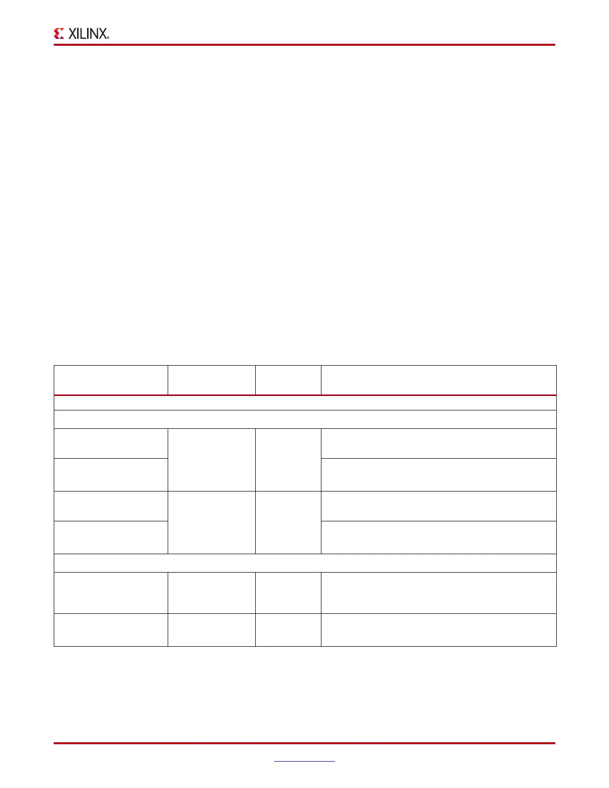
Table 4-25: Block RAM ECC Mode Timing Parameters
Parameter Function
Control
Signal
Description
Setup and Hold Relative to Clock (CLK)
T
RxCK_x
= Setup time (before clock edge) and T
RCKx_x
= Hold time (after clock edge)
T
RDCK_DI_ECC
(Standard ECC Mode)
Data inputs
(1)
DI
Time before the clock that data must be stable at the DI
inputs of the block RAM. Standard ECC mode.
T
RCKD_DI_ECC
(Standard ECC Mode)
Time after the clock that data must be stable at the DI
inputs of the block RAM. Standard ECC mode.
T
RDCK_DI_ECC
(Encode-only Mode)
Data inputs
(1)
DI
Time before the clock that data must be stable at the DI
inputs of the block RAM. Encode-only mode.
T
RCKD_DI_ECC
(Encode-only Mode)
Time after the clock that data must be stable at the DI
inputs of the block RAM. Encode-only mode.
Clock to Out Delays
T
RCKO_DO
(latch mode)
Clock to Output
(2)
CLK to DO Time after the clock that the output data is stable at the
DO outputs of the block RAM (without output
register).
T
RCKO_DO
(register mode)
Clock to Output
(2)
CLK to DO Time after the clock that the output data is stable at the
DO outputs of the block RAM (with output register).
 Loading...


