302 www.xilinx.com Virtex-5 FPGA User Guide
UG190 (v5.0) June 19, 2009
Chapter 6: SelectIO Resources
3.3V I/O Design Guidelines
To achieve maximum performance in Virtex-5 devices, several 3.3V I/O design guidelines
and techniques are highlighted in this section. This includes managing
overshoot/undershoot with termination techniques, regulating V
CCO
at 3.0V with a
voltage regulator, using external bus switches, reviewing configuration methods, and
other design considerations.
I/O Standard Design Rules
Overshoot/Undershoot
Undershoot and overshoot voltages on I/Os operating at 3.3V should not exceed the
absolute maximum ratings of –0.3V to 4.05V, respectively, when V
CCO
is 3.75V. These
absolute maximum limits are stated in the absolute maximum ratings table in the Virtex-5
FPGA Data Sheet. However, the maximum undershoot value is directly affected by the
value of V
CCO
.
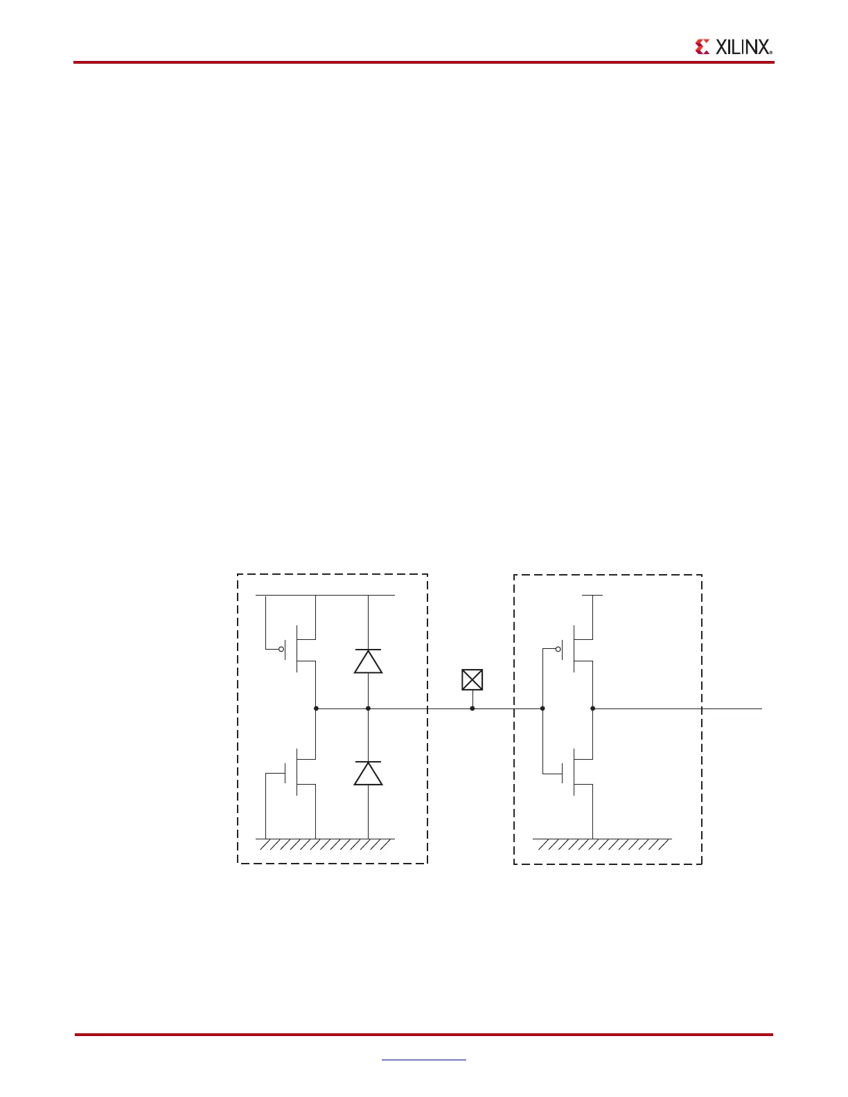
The voltage across the gate oxide at any time must not exceed 4.05V. Consider the case in
which the I/O is either an input or a 3-stated buffer as shown in Figure 6-91. The gate of the
output PMOS transistor P
0
and NMOS transistor N
0
is connected essentially to V
CCO
and
ground, respectively.
The amount of undershoot allowed without overstressing the PMOS transistor P
0
is the
gate voltage minus the gate oxide limit, or V
CCO
– 4.05V.
Similarly, the absolute maximum overshoot allowed without overstressing the NMOS
transistor N
0
is the gate voltage plus the gate oxide limit, or Ground + 4.05V.
The clamp diodes offer protection against transient voltage beyond approximately
V
CCO
+ 0.5V and Ground – 0.5V. The voltage across the diode increases proportionally to
the current going through it. Therefore the clamped level is not fixed and can vary
X-Ref Target - Figure 6-91
Figure 6-91: Virtex-5 FPGA I/O: 3-State Output Driver
ug190_6_85_030506
Output Driver
V
CCO
P
o
N
o
D
G
D
P
N
i
P
i
Power
Clamp
Diode
Ground
Clamp
Diode
GND GND
V
CCO
External
Pin
Input Buffer
 Loading...


