Virtex-5 FPGA User Guide www.xilinx.com 303
UG190 (v5.0) June 19, 2009
Rules for Combining I/O Standards in the Same Bank
depending on the board design. The absolute maximum I/O limits might be exceeded
even if the clamp diode is active.
The IBIS models contain the voltage-current characteristics of the I/O drivers and clamp
diodes.
To verify overshoot and undershoot are within the I/O absolute maximum specifications,
Xilinx recommends proper I/O termination and performing IBIS simulation.
Source Termination and LVDCI_33
In general, the I/O drivers should match the board trace impedance to within ±10% to
minimize overshoot and undershoot. Source termination is often used for unidirectional
interfaces. The DCI feature has built-in source termination on all user output pins. It
compensates for impedance changes due to voltage and/or temperature fluctuations, and
can match the reference resistor values. Assuming the reference resistor values are the
same as the board trace impedance, the output impedance of the driver will closely match
with the board trace.
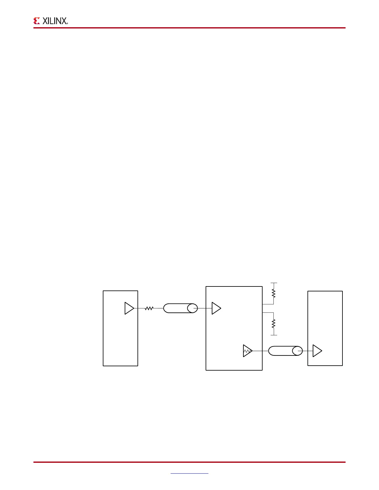
The LVDCI_33 standard is used to enable the DCI features for 3.3V I/O operations. As
shown in Figure 6-92, the OBUF_LVDCI_33 primitive is used to implement the source
termination function in Virtex-5 FPGA output drivers. The pull-up resistor connected to
VRN and the pull-down resistor connected to VRP determine the output impedance of all
the output drivers in the same bank. The “Virtex-5 FPGA Digitally Controlled Impedance
(DCI)” section has more details on using DCI.
Since the LVDCI_33 standard does not offer input termination, source termination must be
implemented on the driver side. Figure 6-92 shows the recommended external source
termination resistors to be incorporated on the external device side.
The total impedance of the LVTTL/LVCMOS driver added to the series termination
resistor R
0
must match the board trace impedance ±10 percent to minimize overshoot and
undershoot. An IBIS simulation is advised for calculating the exact value needed for R
0
.
X-Ref Target - Figure 6-92
Figure 6-92: Connecting LVTTL or LVCMOS Using the LVDCI_33 Standard
R
0
+ R
Driver
=
Z
0
= 50Ω (typical)
Virtex-5 FPGA
Z
0
LVTTL/
LVCMOS
Driver
IBUF_LVDCI_33
Any 3.3V
I/O Device
R
0
V
CCO
= 3.3V
ug190_6_86_030506
Z
0
External Device
OBUF_LVDCI_33
R
REF
V
CCO
VRN
R
REF
VRP
 Loading...


