26 www.xilinx.com Virtex-5 FPGA User Guide
UG190 (v5.0) June 19, 2009
Chapter 1: Clock Resources
Global Clocking Resources
Global clocks are a dedicated network of interconnect specifically designed to reach all
clock inputs to the various resources in an FPGA. These networks are designed to have low
skew and low duty cycle distortion, low power, and improved jitter tolerance. They are
also designed to support very high frequency signals.
Understanding the signal path for a global clock expands the understanding of the various
global clock resources. The global clocking resources and network consist of the following
paths and components:
• Global Clock Inputs
• Global Clock Buffers
• Clock Tree and Nets - GCLK
• Clock Regions
Global Clock Inputs
Virtex-5 FPGAs contain specialized global clock input locations for use as regular user
I/Os if not used as clock inputs. There are 20 global clock inputs per device. Clock inputs
can be configured for any I/O standard, including differential I/O standards. Each clock
input can be either single-ended or differential. All 20 clock inputs can be differential if
desired. When used as outputs, global clock input pins can be configured for any output
standard. Each global clock input pin supports any single-ended output standard or any
output differential standard.
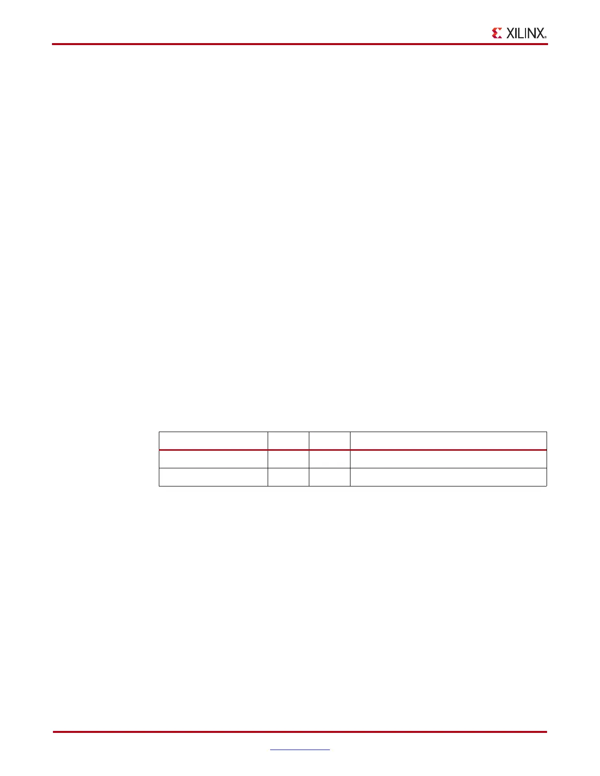
Global Clock Input Buffer Primitives
The primitives in Table 1-1 are different configurations of the input clock I/O input buffer.
These two primitives work in conjunction with the Virtex-5 FPGA I/O resource by setting
the IOSTANDARD attribute to the desired standard. Refer to Chapter 6, “I/O
Compatibility” Table 6-39 for a complete list of possible I/O standards.
Clock Gating for Power Savings
The Virtex-5 FPGA clock architecture provides a straightforward means of implementing
clock gating for the purposes of powering down portions of a design. Most designs contain
several unused BUFGCE resources. A clock can drive a BUFGCE input, and a BUFGCE
output can drive distinct regions of logic. For example, if all the logic that is required to
always be operating is constrained to a few clocking regions, then the BUFGCE output can
drive those regions. Toggling the enable of the BUFGCE provides a simple means of
stopping all dynamic power consumption in the logic regions available for power savings.
The Xilinx Power Estimator (XPE) or the Xilinx Power Analyzer (XPower) tools are used to
estimate power savings. The difference is calculated by setting the frequency on the
corresponding clock net to 0 MHz or providing the appropriate stimulus data to the tool.
Table 1-1: Clock Buffer Primitives
Primitive Input Output Description
IBUFG I O Input clock buffer for single-ended I/O
IBUFGDS I, IB O Input clock buffer for differential I/O
 Loading...


