Virtex-5 FPGA User Guide www.xilinx.com 363
UG190 (v5.0) June 19, 2009
Input Serial-to-Parallel Logic Resources (ISERDES)
ISERDES Latencies
When the ISERDES interface type is MEMORY, the latency through the OCLK stage is one
CLKDIV cycle. However, the total latency through the ISERDES depends on the phase
relationship between the CLK and the OCLK clock inputs. When the ISERDES interface
type is NETWORKING, the latency is two CLKDIV cycles. See Figure 8-12, page 368 and
Figure 8-13, page 369 for a visualization of latency in networking mode. The extra CLKDIV
cycle of latency in networking mode (compared to memory mode) is due to the Bitslip
submodule.
ISERDES Timing Model and Parameters
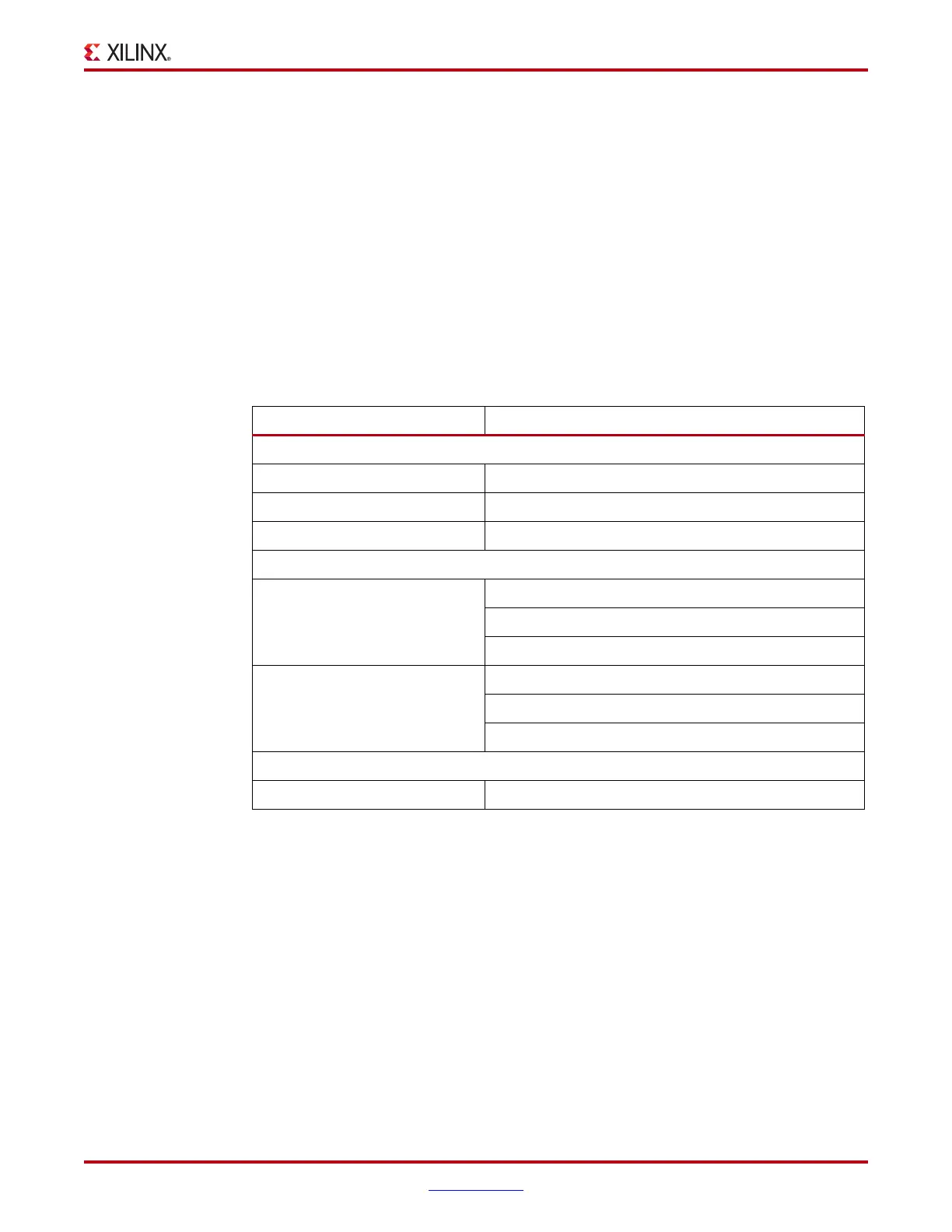
Table 8-4 describes the function and control signals of the ISERDES switching
characteristics in the Virtex-5 FPGA Data Sheet.
Table 8-4: ISERDES Switching Characteristics
Symbol Description
Setup/Hold for Control Lines
T
ISCCK_BITSLIP
/ T
ISCKC_BITSLIP
BITSLIP pin Setup/Hold with respect to CLKDIV
T
ISCCK_CE
/T
ISCKC_CE
CE pin Setup/Hold with respect to CLK (for CE1)
T
ISCCK_CE
/T
ISCKC_CE
CE pin Setup/Hold with respect to CLKDIV (for CE2)
Setup/Hold for Data Lines
T
ISDCK_D
/ T
ISCKD_D
D pin Setup/Hold with respect to CLK
D pin Setup/Hold with respect to CLK
D pin Setup/Hold with respect to CLK
T
ISDCK_DDR
/ T
ISCKD_DDR
D pin Setup/Hold with respect to CLK at DDR mode
D pin Setup/Hold with respect to CLK at DDR mode
D pin Setup/Hold with respect to CLK at DDR mode
Sequential Delay
T
ISCKO_Q
CLKDIV to Out at Q pins
 Loading...


