312 www.xilinx.com Virtex-5 FPGA User Guide
UG190 (v5.0) June 19, 2009
Chapter 6: SelectIO Resources
Actual SSO Limits versus Nominal SSO Limits
The Virtex-5 FPGA SSO limits are defined for a set of nominal system conditions in
Table 6-40. To compute the actual limits for a specific user's system, the “Parasitic Factors
Derating Method (PFDM)” must be used. The PFDM allows the user to account for
differences between actual and nominal PCB power systems, receiver capacitive loading,
and maximum allowable ground bounce or V
CC
bounce. A spreadsheet calculator, “Full
Device SSO Calculator,” automates this process.
Electrical Basis of SSO Noise
SSO noise can manifest as power supply disturbance, in the form of ground bounce or V
CC
bounce. GND and V
CC
bounce is a deviation of the die supply voltage (die GND rail or die
V
CC
rail) with respect to the voltage of the associated PCB supply (PCB GND rail or PCB
V
CC
rail). The deviation of die supplies from PCB supplies comes from the voltage induced
across power system parasitics by supply current transients. One cause of current
transients is output driver switching events. Numerous output switching events occurring
at the same time lead to bigger current transients, and therefore bigger induced voltages
(ground bounce, V
CC
bounce, or rail collapse). Relevant transient current paths exist in the
die, package, and PCB, therefore, parasitics from all three must be considered. The larger
the value of these parasitics, the larger the voltage induced by a current transient (power-
supply disturbance).
V
CC
bounce affects stable high outputs. Ground bounce affects stable low outputs. Ground
bounce also affects inputs configured as certain I/O standards because they interpret
incoming signals by comparing them to a threshold referenced to the die ground (as
opposed to I/O standards with input thresholds referenced to a V
REF
voltage). If the die
voltage disturbance exceeds the instantaneous noise margin for the interface, then a non-
changing input or output can be erroneously interpreted as changing.
SSO noise can also manifest in the form of crosstalk between I/Os in close proximity to one
another. The sparse chevron pinout of Virtex-5 devices reduces crosstalk in the pinout
region to a minimum.
Parasitic Factors Derating Method (PFDM)
This section describes a method to evaluate whether a design is within the SSO limits when
taking into account the specific electrical characteristics of the user's unique system.
The SSO limits in Table 6-40 assume nominal values for the parasitic factors of the system.
These factors fall into three groups of electrical characteristics:
• PCB PDS parasitics (nominal 1 nH per via)
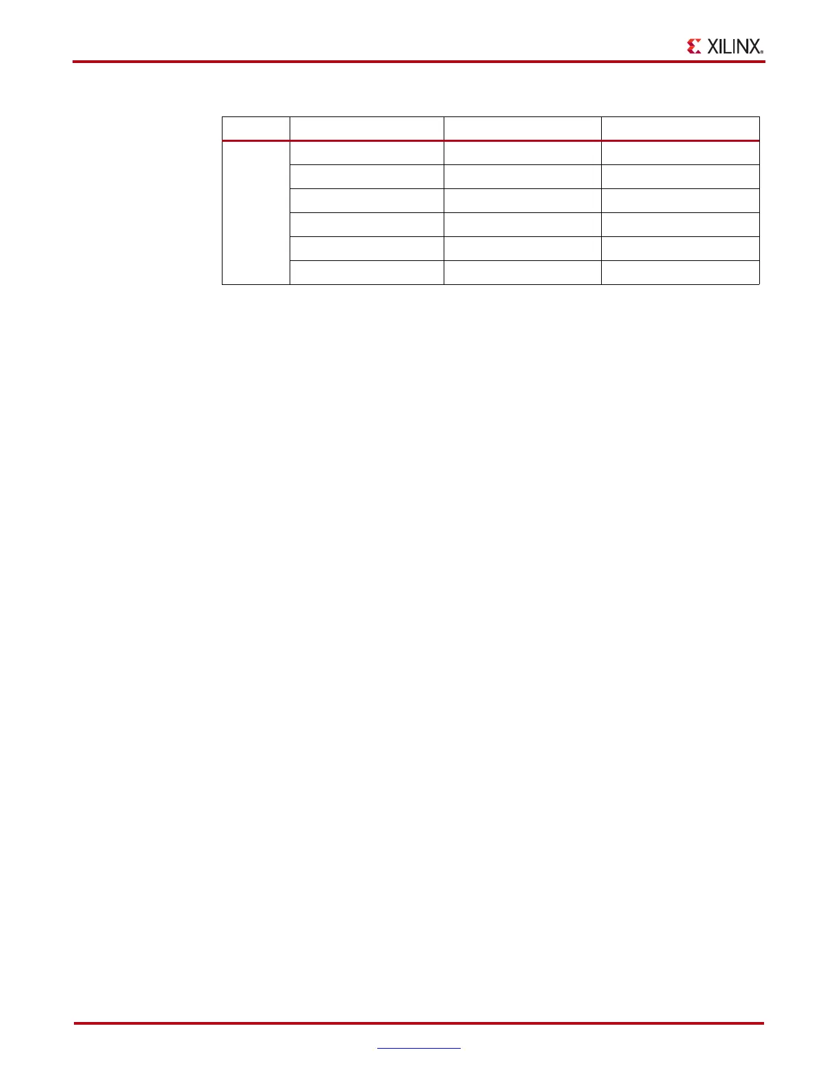
3.3V GTL 12 25
GTL_DCI 12 25
GTLP 12 25
GTLP_DCI 12 25
LVDCI_33 50 Ω 20 40
HSLVDCI_33 50 Ω 20 40
Table 6-40:
Maximum Number of Simultaneously Switching Outputs per Bank (Continued)
Voltage IOSTANDARD Limit per 20-pin Bank Limit per 40-pin Bank
 Loading...


