104 www.xilinx.com Virtex-5 FPGA User Guide
UG190 (v5.0) June 19, 2009
Chapter 3: Phase-Locked Loops (PLLs)
All “O” counters are equivalent, anything O0 can do, O1 can do. The PLL outputs are
flexible when connecting to the global clock network since they are identical. In most cases,
this level of detail is imperceptible to the designer as the software and PLL Wizard
determines the proper settings through the PLL attributes and Wizard inputs.
Reference Clock Switching
The PLL reference clock can be dynamically switched by using the CLKINSEL pin. The
switching is done asynchronously. Since the clock signal can generate a narrow pulse
resulting in erroneous behavior of the PLL, the PLL should be held in RESET while
selecting the alternate clock with the CLKINSEL (CLKSRC) signal. The PLL clock mux
switching is shown in Figure 3-9. The CLKINSEL (CLKSRC) signal directly controls the
mux. No synchronization logic is present.
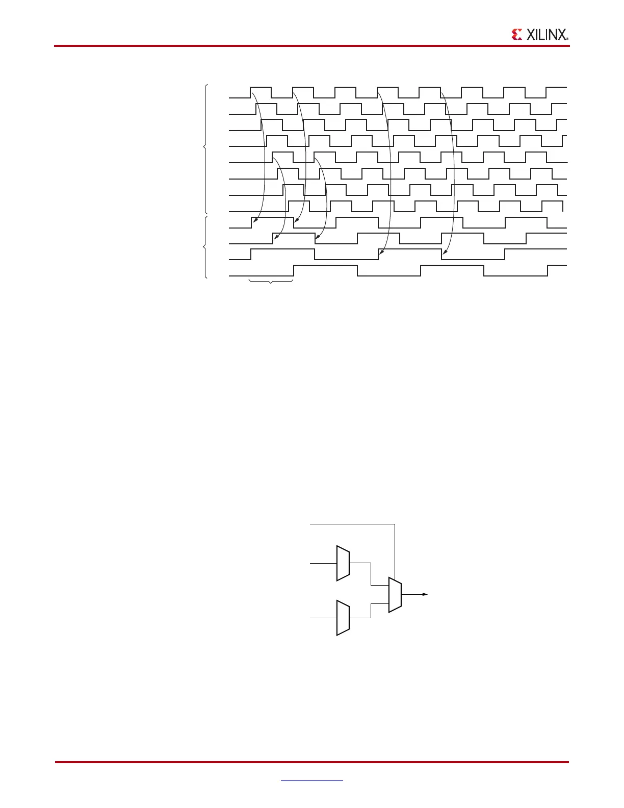
X-Ref Target - Figure 3-8
Figure 3-8: Selecting VCO Phases
One Cycle Delay
Counter
Outputs
VCO
8 Phases
0°
45°
90°
135°
180°
225°
270°
315°
O0
O1
O2
O3
ug190_03_08_032506
X-Ref Target - Figure 3-9
Figure 3-9: Input Clock Switching
BUFG
IBUFG
DCM
BUFG
IBUFG
DCM
CLKIN1
CLKIN2
ug190_3_09_050906
CLKSRC
PLL
CLKIN
 Loading...


