Virtex-5 FPGA User Guide www.xilinx.com 139
UG190 (v5.0) June 19, 2009
Block RAM Retargeting
Block RAM Retargeting
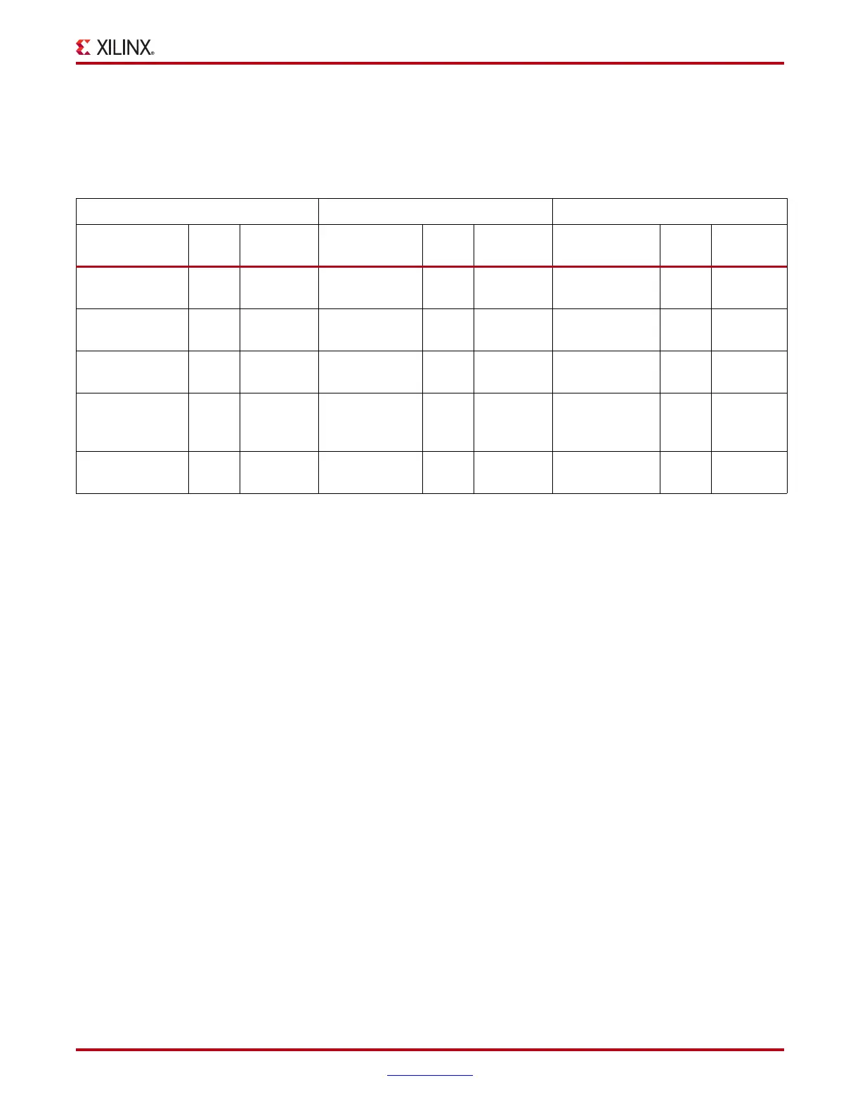
Table 4-12 suggests the most appropriate primitives to choose when mapping a Virtex-4
FPGA block RAM design in a new Virtex-5 FPGA design.
Built-in FIFO Support
Many FPGA designs use block RAMs to implement FIFOs. In the Virtex-5 architecture,
dedicated logic in the block RAM enables users to easily implement synchronous or
multirate (asynchronous) FIFOs. This eliminates the need for additional CLB logic for
counter, comparator, or status flag generation, and uses just one block RAM resource per
FIFO. Both standard and first-word fall-through (FWFT) modes are supported.
In the Virtex-5 architecture, the FIFO can be configured as a 18 Kb or 36 Kb memory. For
the 18 Kb mode, the supported configurations are 4K x 4, 2K x 9, 1K x 18, and 512 x 36. The
supported configurations for the 36 Kb FIFO are 8K x 4, 4K x 9, 2K x 18, 1K x 36, and
512 x 72.
The block RAM can be configured as first-in/first-out (FIFO) memory with common or
independent read and write clocks. Port A of the block RAM is used as a FIFO read port,
and Port B is a FIFO write port. Data is read from the FIFO on the rising edge of read clock
and written to the FIFO on the rising edge of write clock. Independent read and write port
width selection is not supported in FIFO mode without the aid of external CLB logic.
Multirate FIFO
The multirate FIFO offers a very simple user interface. The design relies on free-running
write and read clocks, of identical or different frequencies up to the specified maximum
frequency limit. The design avoids any ambiguity, glitch, or metastable problems, even
when the two frequencies are completely unrelated.
The write operation is synchronous, writing the data word available at DI into the FIFO
whenever WREN is active a set-up time before the rising WRCLK edge.
The read operation is also synchronous, presenting the next data word at DO whenever the
RDEN is active one set-up time before the rising RDCLK edge.
Table 4-12: Block RAM Retargeting
Virtex-4 Block RAM 18k Virtex-5 Block RAM 36k Virtex-5 Block RAM
Primitive Depth
Port Width
R/W
Primitive Depth
Port Width
R/W
Primitive Depth
Port Width
R/W
RAMB16
True dual port
1k to
16k
1, 2, 4, 9, 18 RAMB18 1k to
16k
1, 2, 4, 9, 18 RAMB36 2k to
32k
1, 2, 4, 9, 18
RAMB16
True dual port
512 36/36 N/A N/A N/A RAMB36 1k 36/36
RAMB16
Simple dual port
512 36/36
RAMB18
Simple dual port
512 36/36 RAMB36
Simple dual port
1k 36/36
RAMB16
Simple dual port
Variable Use closest
RAMB18 True
dual-port
N/A N/A Use closest
RAMB36 True
dual port
N/A N/A
CASC of two
RAMB16s
32k 1 N/A N/A N/A RAMB36 32k 1
 Loading...


