Virtex-5 FPGA User Guide www.xilinx.com 381
UG190 (v5.0) June 19, 2009
Output Parallel-to-Serial Logic Resources (OSERDES)
Clock Event 1
T1, T2, and T4 are driven Low to release the 3-state condition. The serialization paths of
T1–T4 and D1–D4 in the OSERDES are identical (including latency), such that the bits
EFGH are always aligned with the 0010 presented at the T1–T4 pins during Clock Event 1.
Clock Event 2
The data bit E appears at OQ one CLK cycle after EFGH is sampled into the OSERDES. This
latency is consistent with the Table 8-10 listing of a 4:1 DDR mode OSERDES latency of one
CLK cycle.
The 3-state bit 0 at T1 during Clock Event 1 appears at TQ one CLK cycle after 0010 is
sampled into the OSERDES 3-state block. This latency is consistent with the Table 8-10
listing of a 4:1 DDR mode OSERDES latency of one CLK cycle.
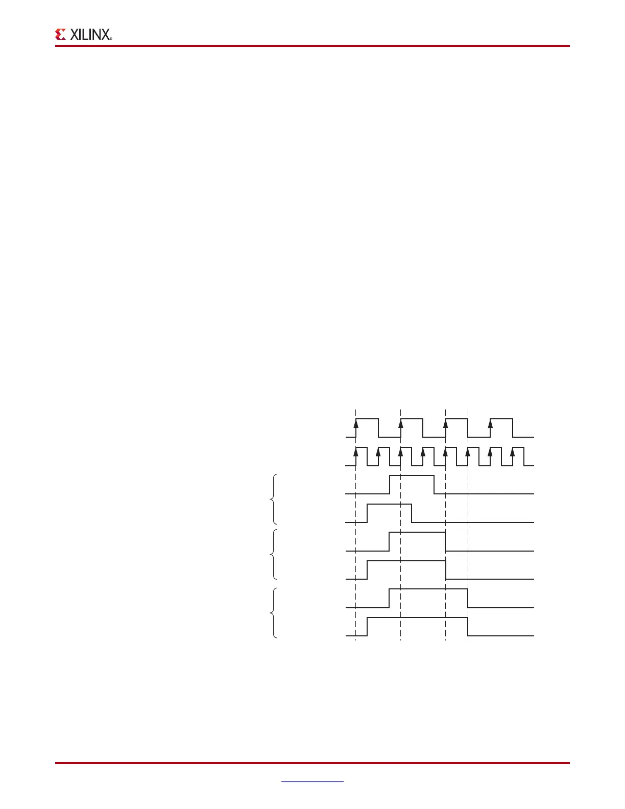
Reset Output Timing
Clock Event 1
A reset pulse is generated on the rising edge of CLKDIV. Because the pulse must take two
different routes to get to OSERDES0 and OSERDES1, there are different propagation
delays for both paths. The difference in propagation delay is emphasized in Figure 8-20.
The path to OSERDES0 is very long and the path to OSERDES1 is very short, such that
each OSERDES receives the reset pulse in a different CLK cycle. The internal resets for both
CLK and CLKDIV go into reset asynchronously when the SR input is asserted.
X-Ref Target - Figure 8-20
Figure 8-20: Two OSERDES Coming Out of Reset Synchronously with One Another
UG070_c8_20_100307
CLKDIV
OSERDES0
Signal at
SR Input
OSERDES1
OSERDES0
OSERDES1
OSERDES0
OSERDES1
CLK
Clock
Event 1
Clock
Event 2
Clock
Event 3
Clock
Event 4
Internal Reset
(CLKDIV)
Internal Reset
(CLK)
 Loading...


