Virtex-5 FPGA User Guide www.xilinx.com 41
UG190 (v5.0) June 19, 2009
Regional Clocking Resources
I/O Clock Buffer - BUFIO
The I/O clock buffer (BUFIO) is a clock buffer available in Virtex-5 devices. The BUFIO
drives a dedicated clock net within the I/O column, independent of the global clock
resources. Thus, BUFIOs are ideally suited for source-synchronous data capture
(forwarded/receiver clock distribution). BUFIOs can only be driven by clock capable I/Os
located in the same clock region. In a typical clock region, there are four BUFIOs. Each
BUFIO can drive a single I/O clock network in the same region/bank, as well as the
regional clock buffers (BUFR). BUFIOs cannot drive logic resources (CLB, block RAM,
IODELAY, etc.) because the I/O clock network only reaches the I/O column in the same
bank or clock region.
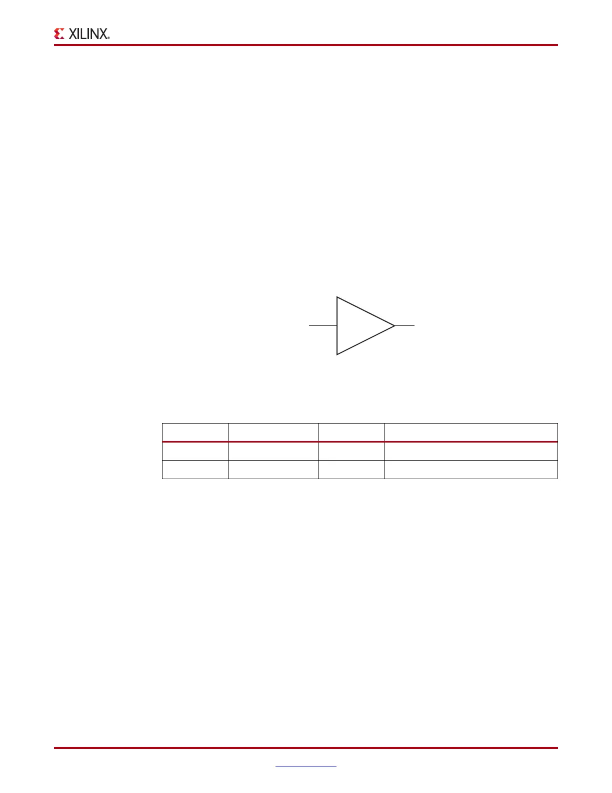
BUFIO Primitive
BUFIO is simply a clock in, clock out buffer. There is a phase delay between input and
output. Figure 1-18 shows the BUFIO. Table 1-6 lists the BUFIO ports. A location constraint
is available for BUFIO.
BUFIO Use Models
In Figure 1-19, a BUFIO is used to drive the I/O logic using the clock capable I/O. This
implementation is ideal in source-synchronous applications where a forwarded clock is
used to capture incoming data.
X-Ref Target - Figure 1-18
Figure 1-18: BUFIO Primitive
Table 1-6: BUFIO Port List and Definitions
Port Name Type Width Definition
O Output 1 Clock output port
I Input 1 Clock input port
BUFIO
ug190_1_18_032306
O
I
 Loading...


