Virtex-5 FPGA User Guide www.xilinx.com 103
UG190 (v5.0) June 19, 2009
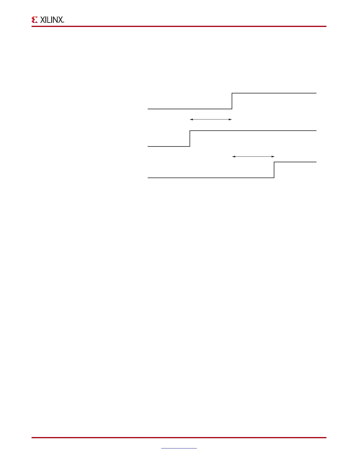
Detailed VCO and Output Counter Waveforms
Clock Shifting
The PLL output clocks can be shifted by inserting delay by selecting one of the eight phases
in either the reference or the feedback path. Figure 3-7 shows the effect on a clock signal
edge at the output of the PLL without any shifting versus the two cases (delay inserted in
the feedback path and delay inserted in the reference path).
Detailed VCO and Output Counter Waveforms
Figure 3-8 shows the eight VCO phase outputs and four different counter outputs. Each
VCO phase is shown with the appropriate start-up sequence. The phase relationship and
start-up sequence are guaranteed to insure the correct phase is maintained. This means the
rising edge of the 0° phase will happen before the rising edge of the 45° phase. The O0
counter is programmed to do a simple divide by two with the 0° phase tap as the reference
clock. The O1 counter is programmed to do a simple divide by two but uses the 180° phase
tap from the VCO. Phase shifts greater than one VCO period are possible. This counter
setting could be used to generate a clock for a DDR interface where the reference clock is
edge aligned to the data transition. The O2 counter is programmed to do a divide by three.
The O3 output has the same programming as the O2 output except the phase is set for a
one cycle delay.
If the PLL is configured to provide a certain phase relationship and the input frequency is
changed, then this phase relationship is also changed since the VCO frequency changes
and therefore the absolute shift in picoseconds will change. This aspect must be considered
when designing with the PLL. When an important aspect of the design is to maintain a
certain phase relationship amongst various clock outputs, (e.g., CLK and CLK90) then this
relationship will be maintained regardless of the input frequency.
X-Ref Target - Figure 3-7
Figure 3-7: Basic Output Clock Shifting
original
clock
added delay in
feedback path
added delay in
reference path
dT
reference
dT
feedback
ug190_03_07_032506
 Loading...


