Virtex-5 FPGA User Guide www.xilinx.com 247
UG190 (v5.0) June 19, 2009
Specific Guidelines for I/O Supported Standards
PCI-X, PCI-33, PCI-66 (Peripheral Component Interconnect)
The PCI™ standard specifies support for 33 MHz and 66 MHz bus applications. The
PCI-X™ standard specifies support for 66 MHz and 133 MHz bus applications. These
standards use an LVTTL input buffer and a push-pull output buffer. These standards do
not require the use of a reference voltage (V
REF
) or a board termination voltage (V
TT
).
However, they do require 3.3V input/output source voltage (V
CCO
).
A PCI undershoot/overshoot specification could require V
CCO
to be regulated at 3.0V as
discussed in “Regulating V
CCO
at 3.0V,” page 304. This is not necessary if overshoot and
undershoot are controlled by careful design.
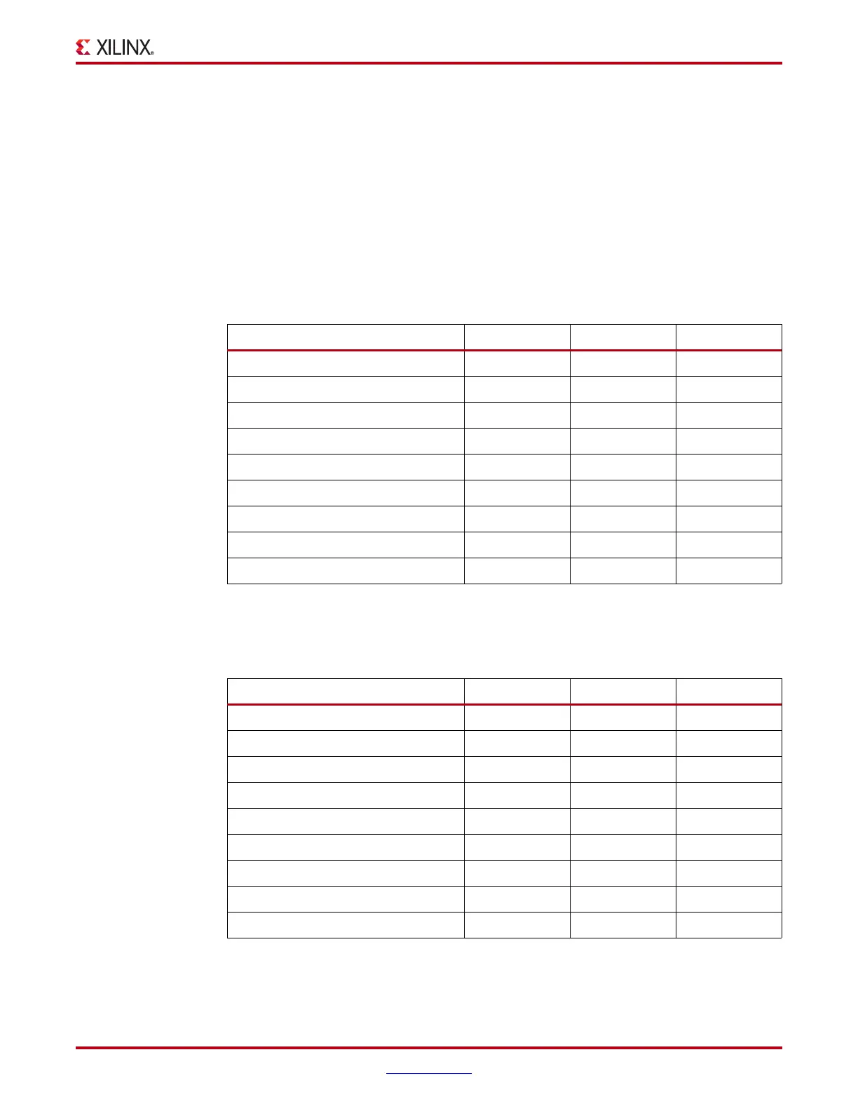
Table 6-11 and Table 6-12 lists the DC voltage specifications.
Table 6-11: PCI33_3, PCI66_3 Voltage Specifications
(2)
Parameter Min Typ Max
V
CCO
3.0 3.3 3.5
V
REF
– – –
V
TT
– – –
V
IH
= 0.5 × V
CCO
1.5 1.65 V
CCO
V
IL
= 0.3 × V
CCO
–0.20.991.05
V
OH
= 0.9 × V
CCO
2.7 – –
V
OL
= 0.1 × V
CCO
– – 0.35
I
OH
at V
OH
(mA) (Note 1) – –
I
OL
at V
OL
(mA) (Note 1) – –
Notes:
1. Tested according to the relevant specification.
2. For complete specifications, refer to the PCI specification.
Table 6-12: PCI-X DC Voltage Specifications
(2)
Parameter Min Typ Max
V
CCO
3.0 3.3 3.5
V
REF
– – –
V
TT
– – –
V
IH
= 0.5 × V
CCO
1.5 1.65 V
CCO
V
IL
= 0.35 × V
CCO
–0.2 1.155 1.225
V
OH
= 0.9 × V
CCO
2.7 – –
V
OL
= 0.1 × V
CCO
– – 0.35
I
OH
at V
OH
(mA) (Note 1) – –
I
OL
at V
OL
(mA) (Note 1) – –
Notes:
1. Tested according to the relevant specification.
2. For complete specifications, refer to the PCI-X specification.
 Loading...


