Virtex-5 FPGA User Guide www.xilinx.com 51
UG190 (v5.0) June 19, 2009
DCM Ports
DCM_ADV Primitive
The DCM_ADV primitive has access to all DCM features and ports available in
DCM_BASE plus additional ports for the dynamic reconfiguration feature. It is a superset
of the DCM_BASE primitive. DCM_ADV uses all the DCM features including clock
deskew, frequency synthesis, fixed or variable phase shifting, and dynamic
reconfiguration. Table 2-3 lists the available ports in the DCM_ADV primitive.
DCM Ports
There are four types of DCM ports available in the Virtex-5 architecture:
• DCM Clock Input Ports
• DCM Control and Data Input Ports
• DCM Clock Output Ports
• DCM Status and Data Output Ports
DCM Clock Input Ports
Source Clock Input - CLKIN
The source clock (CLKIN) input pin provides the source clock to the DCM. The CLKIN
frequency must fall in the ranges specified in the Virtex-5 FPGA Data Sheet. The clock input
signal comes from one of the following buffers:
1. IBUFG – Global Clock Input Buffer
The DCM compensates for the clock input path when CLKFB is connected and an
IBUFG on the same half (top or bottom) of the device as the DCM is used.
2. BUFGCTRL – Internal Global Clock Buffer
Any BUFGCTRL can drive any DCM in the Virtex-5 device using dedicated global
routing. A BUFGCTRL can drive the DCM CLKIN pin when used to connect two
DCMs in series.
3. PLL – Phase-Locked Loop
A PLL block within the same CMT can drive the CLKIN input of either DCM in the
CMT block. No global buffer is required in between. See “Application Examples,”
page 75 for more information.
4. IBUF – Input Buffer
When an IBUF drives the CLKIN input, the PAD to DCM input skew is not
compensated.
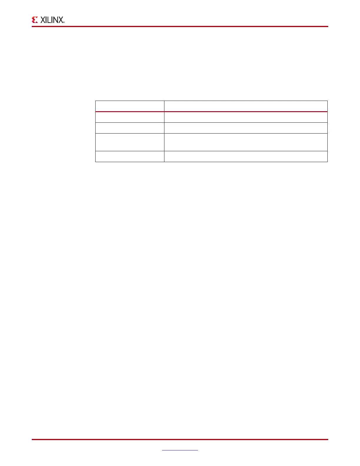
Table 2-3: DCM_ADV Primitive
Available Ports Port Names
Clock Input CLKIN, CLKFB, PSCLK, DCLK
Control and Data Input RST, PSINCDEC, PSEN, DADDR[6:0], DI[15:0], DWE, DEN
Clock Output CLK0, CLK90, CLK180, CLK270, CLK2X, CLK2X180, CLKDV,
CLKFX, CLKFX180
Status and Data Output LOCKED, PSDONE, DO[15:0], DRDY
 Loading...


