Virtex-5 FPGA User Guide www.xilinx.com 307
UG190 (v5.0) June 19, 2009
Simultaneous Switching Output Limits
Nominal SSO Limit
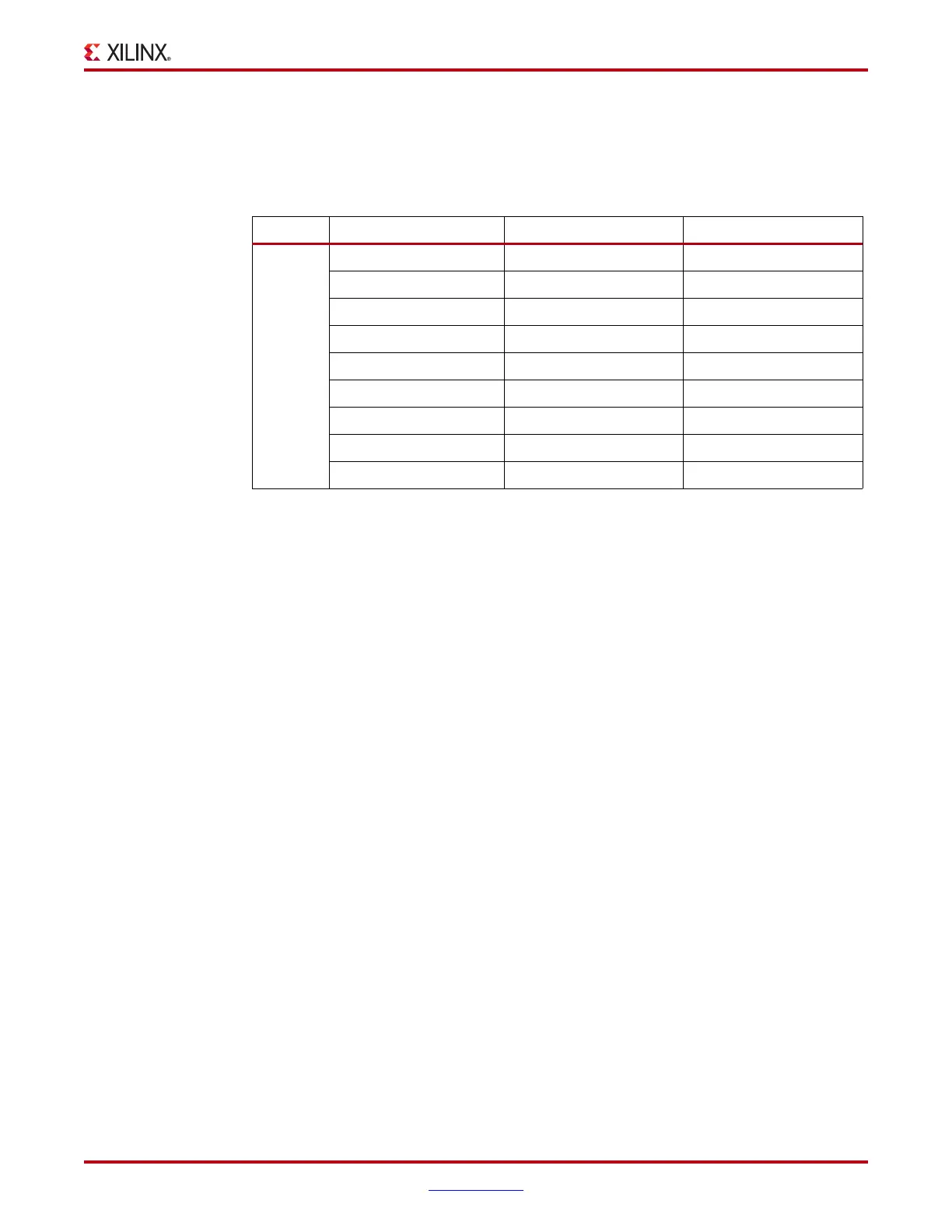
Table 6-40 provides the guidelines for the maximum number of simultaneously switching
outputs allowed per bank to avoid the effects of ground bounce.
Table 6-40:
Maximum Number of Simultaneously Switching Outputs per Bank
Voltage IOSTANDARD Limit per 20-pin Bank Limit per 40-pin Bank
1.2V HSTL_I_12 20 40
LVCMOS12_2_slow 20 40
LVCMOS12_4_slow 20 40
LVCMOS12_6_slow 20 40
LVCMOS12_8_slow 20 40
LVCMOS12_2_fast 20 40
LVCMOS12_4_fast 20 40
LVCMOS12_6_fast 20 40
LVCMOS12_8_fast 20 40
 Loading...


