130 www.xilinx.com Virtex-5 FPGA User Guide
UG190 (v5.0) June 19, 2009
Chapter 4: Block RAM
Output Latches/Registers Synchronous Set/Reset (SRVAL_[A|B])
The SRVAL (single-port) or SRVAL_A and SRVAL_B (dual-port) attributes define output
latch values when the SSR input is asserted. The width of the SRVAL (SRVAL_A and
SRVAL_B) attribute is the port width, as shown in Table 4-10. These attributes are hex-
encoded bit vectors and the default value is 0. This attribute sets the value of the output
register when the optional output register attribute is set. When the register is not used, the
latch gets set to the SRVAL instead. In the 36-bit mode, SRVAL[35:32] corresponds to
DP[3:0].
Optional Output Register On/Off Switch - DO[A|B]_REG
This attribute sets the number of pipeline register at A/B output of the block RAM. The
valid values are 0 (default) or 1.
Extended Mode Address Determinant - RAM_EXTENSION_[A|B]
This attribute determines whether the block RAM of interest has its A/B port as
UPPER/LOWER address when using the cascade mode. Refer to the “Cascadable Block
RAM” section. When the block RAM is not used in cascade mode, the default value is
NONE.
Read Width - READ_WIDTH_[A|B]
This attribute determines the A/B read port width of the block RAM. The valid values are:
0 (default), 1, 2, 4, 9, 18, and 36.
Write Width - WRITE_WIDTH_[A|B]
This attribute determines the A/B write port width of the block RAM. The valid values are:
0 (default), 1, 2, 4, 9, 18, and 36.
Write Mode - WRITE_MODE_[A|B]
This attribute determines the write mode of the A/B input ports. The possible values are
WRITE_FIRST (default), READ_FIRST, and NO_CHANGE. Additional information on the
write modes is in the “Write Modes” section.
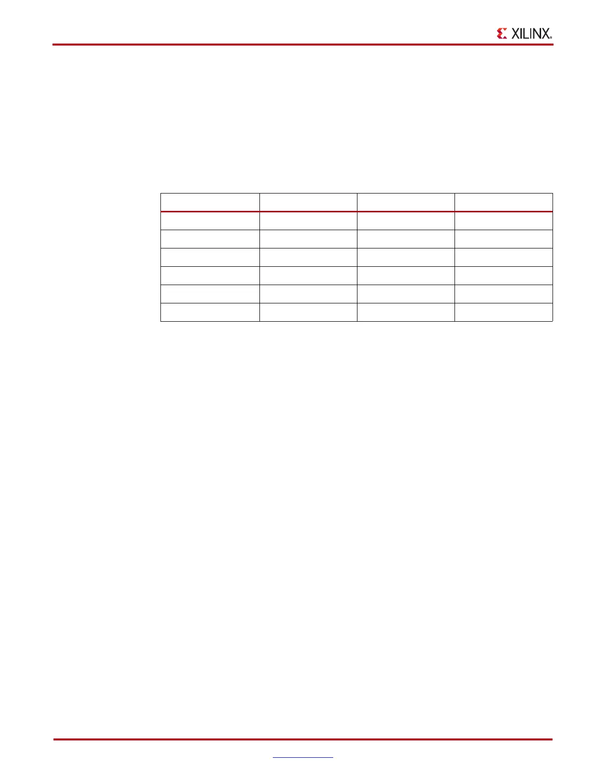
Table 4-10: Port Width Values
Port Data Width DOP Bus DO Bus INIT / SRVAL
1 NA <0> 1
2 NA <1:0> 2
4 NA <3:0> 4
9 <0> <7:0> (1 + 8) = 9
18 <1:0> <15:0> (2 + 16) = 18
36 <3:0> <31:0> (4 + 32) = 36
 Loading...


