Virtex-5 FPGA User Guide www.xilinx.com 239
UG190 (v5.0) June 19, 2009
Specific Guidelines for I/O Supported Standards
Specific Guidelines for I/O Supported Standards
The following subsections provide an overview of the I/O standards supported by all
Virtex-5 devices.
While most Virtex-5 FPGA I/O supported standards specify a range of allowed voltages,
this chapter records typical voltage values only. Detailed information on each specification
can be found on the Electronic Industry Alliance JEDEC web site at http://www.jedec.org.
LVTTL (Low Voltage Transistor-Transistor Logic)
The low-voltage TTL (LVTTL) standard is a general purpose EIA/JESDSA standard for
3.3V applications using an LVTTL input buffer and a push-pull output buffer. This
standard requires a 3.3V input and output supply voltage (V
CCO
), but does not require the
use of a reference voltage (V
REF
) or a termination voltage (V
TT
).
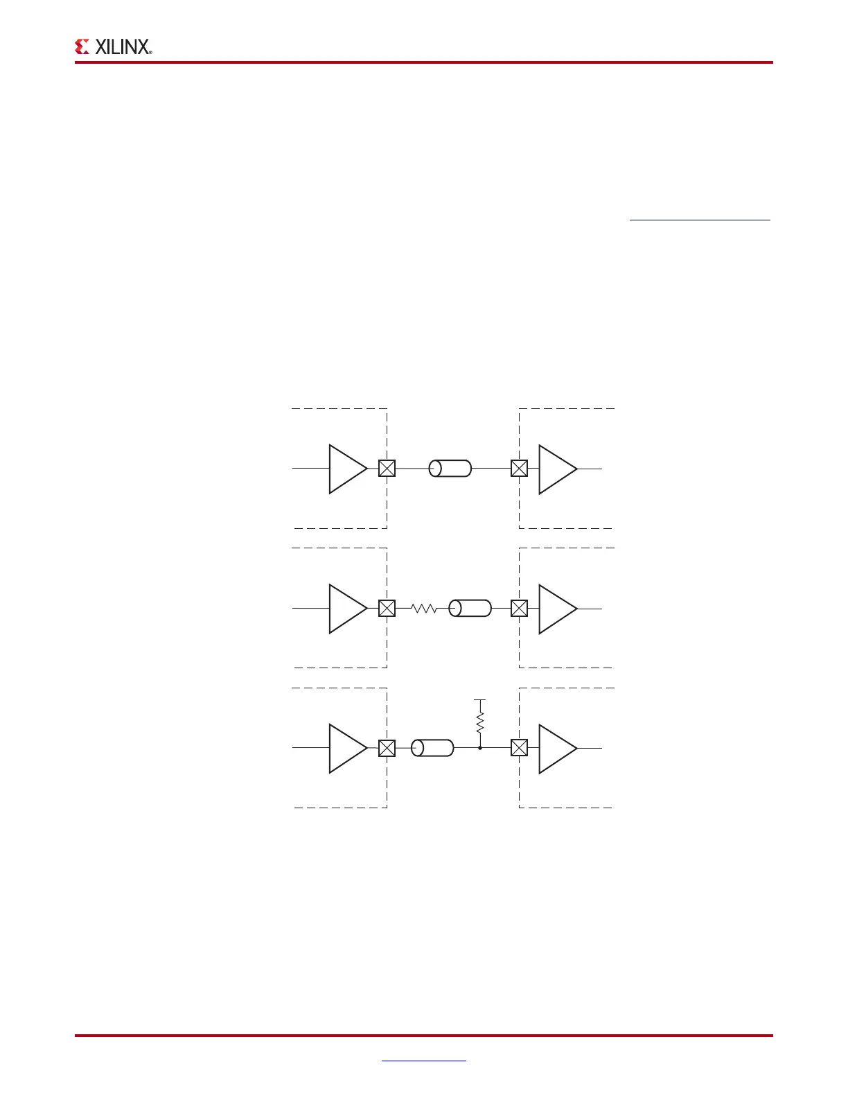
Sample circuits illustrating both unidirectional and bidirectional LVTTL termination
techniques are shown in Figure 6-27 and Figure 6-28.
X-Ref Target - Figure 6-27
Figure 6-27: LVTTL Unidirectional Termination
Z
0
IOB
IOB
LVT T L
LVT T L
Z
0
IOB
IOB
LVT T L
LVT T L
Z
0
IOB
IOB
LVT T L
LVT T L
ug190_6_24_022806
V
TT
Note: V
TT
is any voltage from 0V to V
CCO
R
P
= Z
0
R
S
= Z
0
– R
D
 Loading...


