330 www.xilinx.com Virtex-5 FPGA User Guide
UG190 (v5.0) June 19, 2009
Chapter 7: SelectIO Logic Resources
ODELAY_VALUE Attribute
The ODELAY_VALUE attribute specifies tap delays. The possible values are any integer
from 0 to 63. The default value is zero. The value of the tap delay reverts to
ODELAY_VALUE when the tap delay is reset.
HIGH_PERFORMANCE_MODE Attribute
When TRUE, this attribute reduces the output jitter. This reduction results in a slight
increase in power dissipation from the IODELAY element. When set to FALSE the
IODELAY element consumes less power.
SIGNAL_PATTERN Attribute
Clock and data signals have different electrical profiles and therefore accumulate different
amounts of jitter in the IODELAY chain. By setting the SIGNAL_PATTERN attribute, the
user enables timing analyzer to account for jitter appropriately when calculating timing. A
clock signal is periodic in nature and does not have long sequences of consecutive ones or
zeroes, while data is random in nature and can have long and short sequences of ones and
zeroes.
IODELAY Timing
Table 7-11 shows the IODELAY switching characteristics.
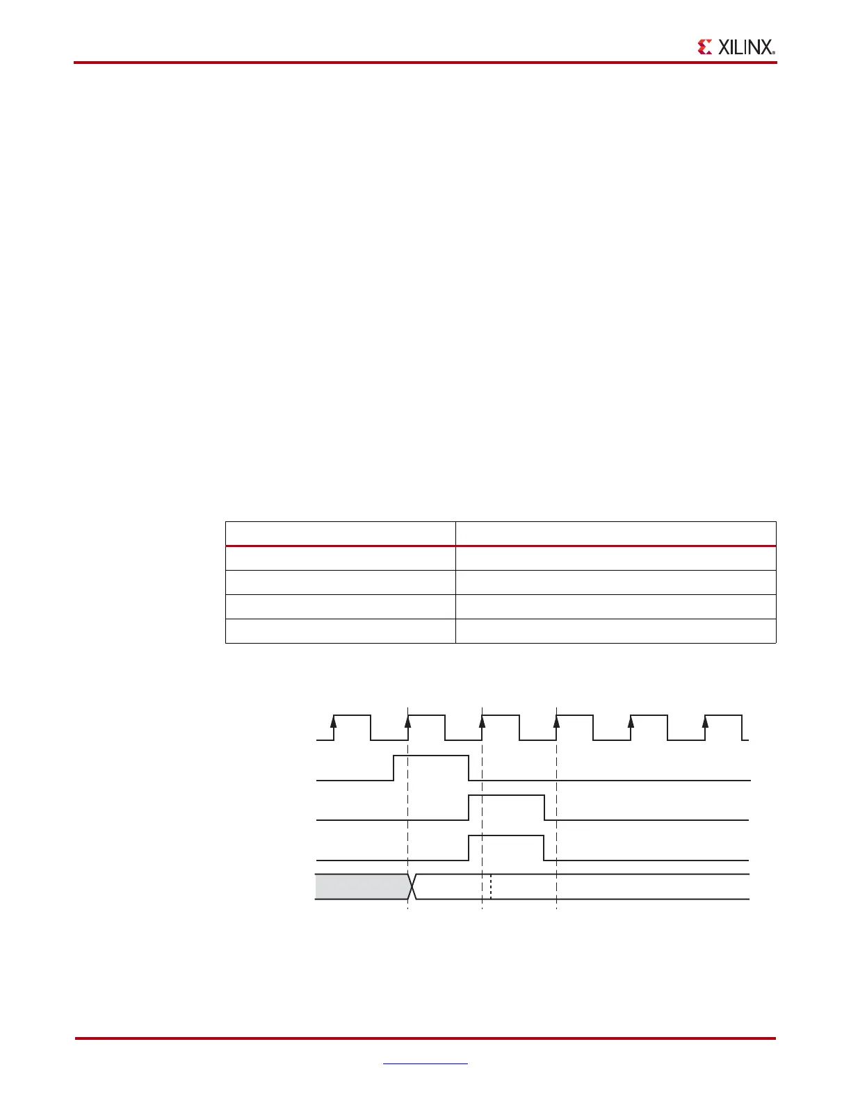
Figure 7-9 shows an IDELAY timing diagram. It is assumed that IDELAY_VALUE = 0.
Table 7-11: IODELAY Switching Characteristics
Symbol Description
T
IDELAYRESOLUTION
IDELAY tap resolution
T
ICECK
/T
ICKCE
CE pin Setup/Hold with respect to C
T
IINCCK
/T
ICKINC
INC pin Setup/Hold with respect to C
T
IRSTCK
/T
ICKRST
RST pin Setup/Hold with respect to C
X-Ref Target - Figure 7-9
Figure 7-9: IDELAY Timing Diagram
UG190_7_09_100107
RST
C
123
CE
INC
DATAOUT
Tap 0 Tap 1
 Loading...


