Virtex-5 FPGA User Guide www.xilinx.com 369
UG190 (v5.0) June 19, 2009
Input Serial-to-Parallel Logic Resources (ISERDES)
Clock Event 4
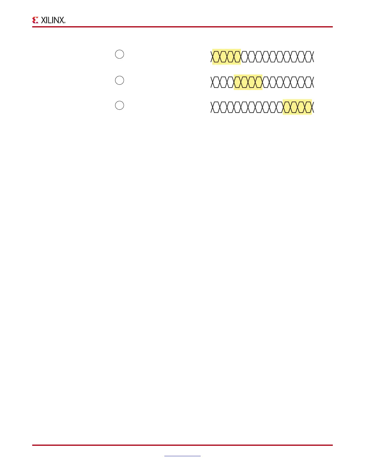
The first two bits of the fourth word CD have been sampled into the input side registers of
the ISERDES. On this same edge of CLKDIV, the second word sampled is presented to
Q1–Q4 with one bit shifted to the right. The actual bits from the input stream that appear
at the Q1–Q4 outputs during this cycle are shown in B of Figure 8-13.
The realigned bits on Q1–Q4 are sampled into the FPGA logic on the CLKDIV domain. The
total latency from when the ISERDES captures the asserted Bitslip input to when the
realigned ISERDES outputs Q1–Q4 are sampled by CLKDIV is two CLKDIV cycles.
Clock Event 5
The third word sampled is presented to Q1–Q4 with three bits shifted to the left. The actual
bits from the input stream that appear at the Q1–Q4 outputs during this cycle are shown in
C of Figure 8-13.
X-Ref Target - Figure 8-13
Figure 8-13: Bits from Data Input Stream (D) of Figure 8-12
ug190_c8_13_100307
C
(2nd Bitslip, Rotate 3 Bits to Left)
Q1–Q4 During Clock Event 5
B
(1st Bitslip, Rotate 1 Bit to Right)
Q1–Q4 During Clock Event 4
CDABCD CDABCDAB
CDABCD CDABCDAB
CDABCD CDABCDAB
A
(No Bitslip)
Q1–Q4 During Clock Event 3
 Loading...


