Virtex-5 FPGA User Guide www.xilinx.com 299
UG190 (v5.0) June 19, 2009
Rules for Combining I/O Standards in the Same Bank
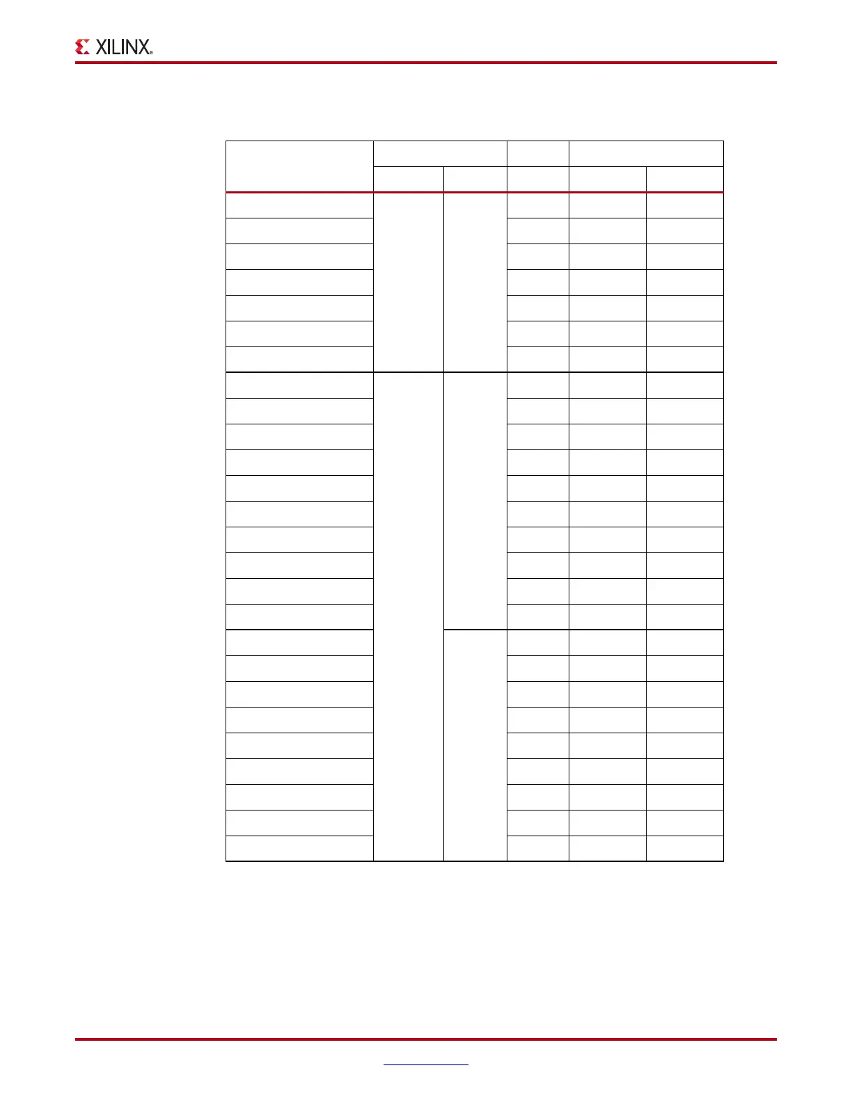
Table 6-39 summarizes the Virtex-5 FPGA supported I/O standards.
Table 6-39: I/O Compatibility
I/O Standard
V
CCO
V
REF
Termination Type
Output Input Input Output Input
LVTTL
(1)
3.3 3.3 N/R N/R N/R
LVCMOS33
(1)
N/R N/R N/R
LVDCI_33
(1)
N/R Series N/R
HSLVDCI_33
(1)
V
CCO
/2 Series N/R
PCIX
(1)
N/R N/R N/R
PCI33_3
(1)
N/R N/R N/R
PCI66_3
(1)
N/R N/R N/R
LVDS_25 2.5 Note (2) N/R N/R N/R
LVDSEXT_25 N/R N/R N/R
HT_25 N/R N/R N/R
RSDS_25
(4)
N/R N/R N/R
BLVDS_25 N/R N/R N/R
LVPECL_25 N/R N/R N/R
SSTL2_I 1.25 N/R N/R
SSTL2_II 1.25 N/R N/R
DIFF_SSTL2_I N/R N/R N/R
DIFF_SSTL2_II N/R N/R N/R
LVCMOS25 2.5 N/R N/R N/R
LVDCI_25 N/R Series N/R
HSLVDCI_25 V
CCO
/2 Series N/R
LVDCI_DV2_25 N/R Series N/R
SSTL2_I_DCI 1.25 N/R Split
SSTL2_II_DCI 1.25 Split Split
SSTL2_II_T_DCI 1.25 N/R Split
DIFF_SSTL2_I_DCI N/R N/R Split
DIFF_SSTL2_II_DCI N/R Split Split
 Loading...


