Virtex-5 FPGA User Guide www.xilinx.com 301
UG190 (v5.0) June 19, 2009
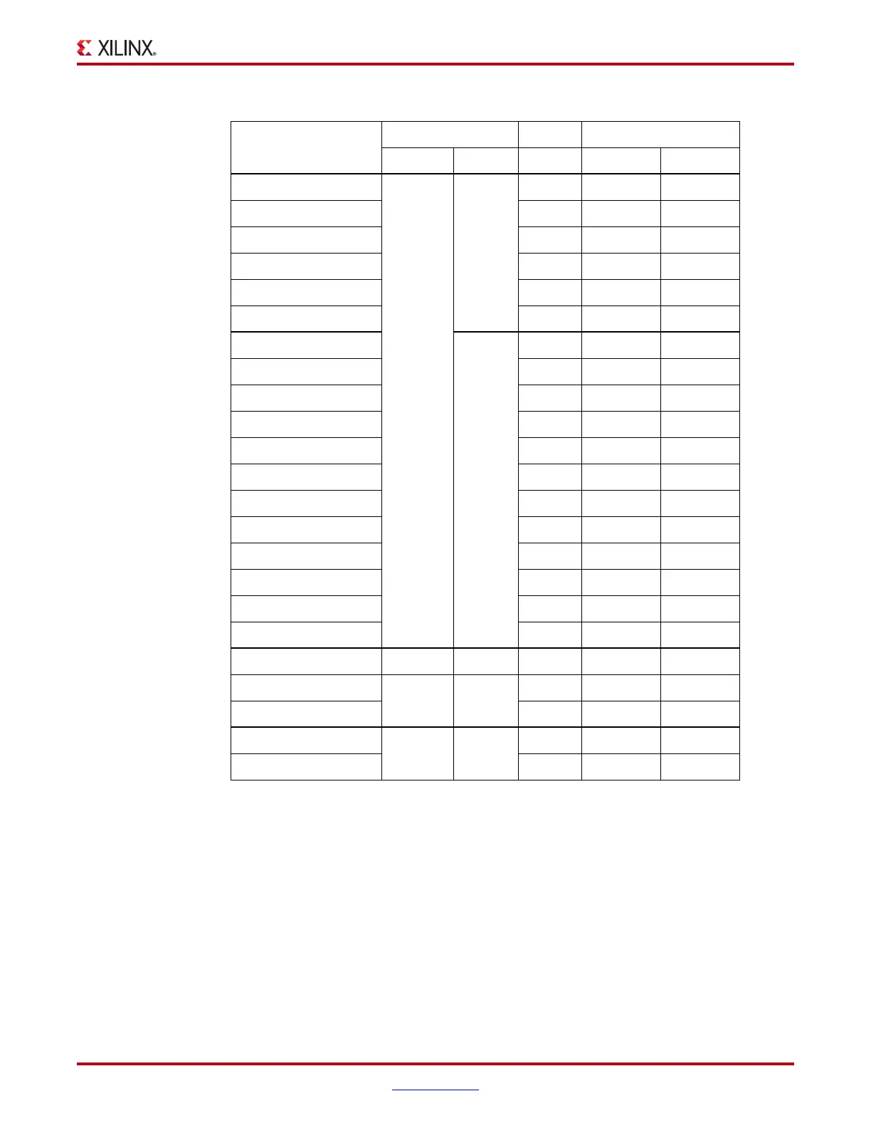
Rules for Combining I/O Standards in the Same Bank
HSTL_III 1.5 Note (2) 0.9 N/R N/R
HSTL_IV 0.9 N/R N/R
HSTL_I 0.75 N/R N/R
HSTL_II 0.75 N/R N/R
DIFF_HSTL_I N/R N/R N/R
DIFF_HSTL_II N/R N/R N/R
LVCMOS15 1.5 N/R N/R N/R
LVDCI_15 N/R Series N/R
HSLVDCI_15 V
CCO
/2 Series N/R
LVDCI_DV2_15 N/R Series N/R
GTLP_DCI 1 Single Single
HSTL_III_DCI 0.9 N/R Single
HSTL_IV_DCI 0.9 Single Single
HSTL_I_DCI 0.75 N/R Split
HSTL_II_DCI 0.75 Split Split
HSTL_II_T_DCI 0.75 N/R Split
DIFF_HSTL_I_DCI N/R N/R Split
DIFF_HSTL_II_DCI N/R Split Split
GTL_DCI 1.2 1.2 0.8 Single Single
GTLP N/R Note (2) 1 N/R N/R
GTL 0.8 N/R N/R
LVCMOS12
1.2 1.2
N/R N/R N/R
HSTL_I_12 0.6 N/R N/R
Notes:
1. See “3.3V I/O Design Guidelines” for more detailed information
2. Differential inputs and inputs using V
REF
are powered from V
CCAUX
. However, pin voltage
must not exceed V
CCO
, due to the presence of clamp diodes to V
CCO
.
3. N/R = no requirement.
4. RSDS_25 has the same DC specifications as LVDS_25. All information pertaining to LVDS_25
is applicable to RSDS_25.
5. I/O standard is selected using the IOSTANDARD attribute.
Table 6-39: I/O Compatibility (Continued)
I/O Standard
V
CCO
V
REF
Termination Type
Output Input Input Output Input
 Loading...


