350 www.xilinx.com Virtex-5 FPGA User Guide
UG190 (v5.0) June 19, 2009
Chapter 7: SelectIO Logic Resources
Clock Event 9
At time T
OSRCK
before Clock Event 9 (rising edge of CLK), the SR signal (configured as
synchronous reset in this case) becomes valid-High resetting ODDR register, reflected at
the OQ output at time T
RQ
after Clock Event 9 (no change at the OQ output in this case)
and resetting ODDR register, reflected at the OQ output at time T
RQ
after Clock Event 10
(no change at the OQ output in this case).
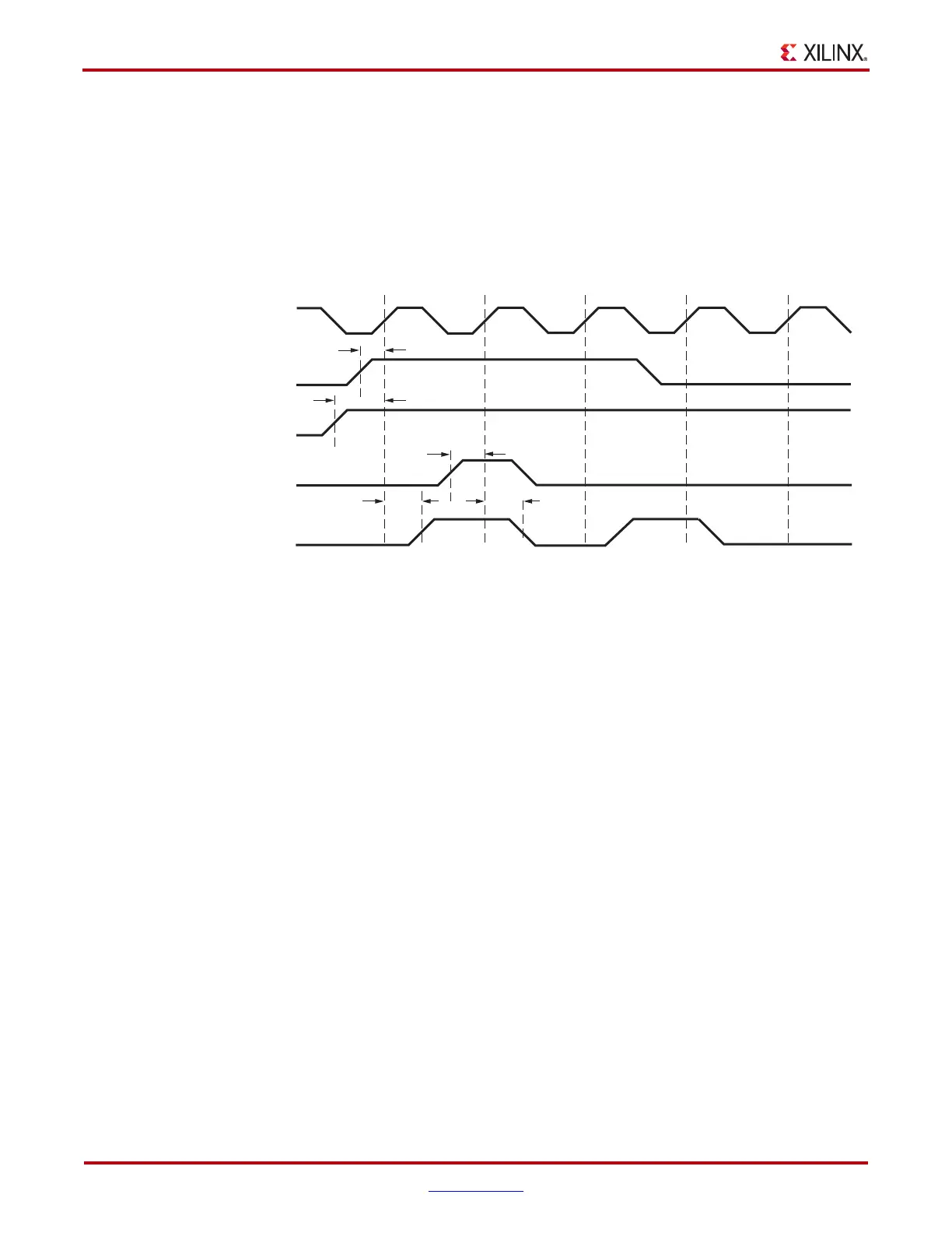
Figure 7-28 illustrates the OLOGIC 3-state register timing.
Clock Event 1
• At time T
OTCECK
before Clock Event 1, the 3-state clock enable signal becomes valid-
High at the TCE input of the 3-state register, enabling the 3-state register for incoming
data.
• At time T
OTCK
before Clock Event 1 the 3-state signal becomes valid-High at the T
input of the 3-state register, returning the pad to high-impedance at time T
OCKQ
after
Clock Event 1.
Clock Event 2
• At time T
OSRCK
before Clock Event 2, the SR signal (configured as synchronous reset
in this case) becomes valid-High, resetting the 3-state register at time T
RQ
after Clock
Event 2.
Figure 7-29 illustrates IOB DDR 3-state register timing. This example is shown using DDR
in opposite edge mode. For other modes add the appropriate latencies as shown in
Figure 7-4, page 321.
X-Ref Target - Figure 7-28
Figure 7-28: OLOGIC 3-State Register Timing Characteristics
12345
CLK
T1
TCE
SR
TQ
T
OCKQ
T
RQ
T
OTCK
T
OTCECK
T
OSRCK
UG190_7_23_041106
 Loading...


