Virtex-5 FPGA User Guide www.xilinx.com 351
UG190 (v5.0) June 19, 2009
OLOGIC Resources
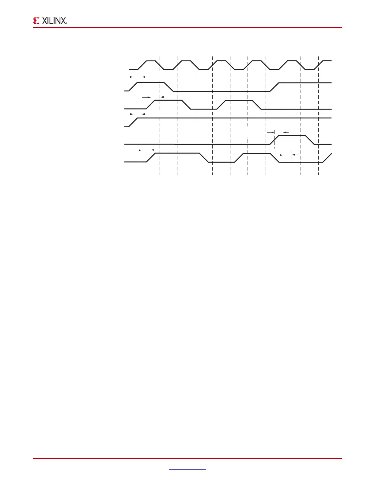
Clock Event 1
• At time T
OTCECK
before Clock Event 1, the 3-state clock enable signal becomes valid-
High at the TCE input of the 3-state ODDR register, enabling them for incoming data.
Care must be taken to toggle the TCE signal of the 3-state ODDR between the rising
edges and falling edges of CLK as well as meeting the register setup-time relative to
both clock edges.
• At time T
OTCK
before Clock Event 1 (rising edge of CLK), the 3-state signal T1
becomes valid-High at the T1 input of 3-state register and is reflected on the TQ
output at time T
OCKQ
after Clock Event 1.
Clock Event 2
• At time T
OTCK
before Clock Event 2 (falling edge of CLK), the 3-state signal T2
becomes valid-High at the T2 input of 3-state register and is reflected on the TQ
output at time T
OCKQ
after Clock Event 2 (no change at the TQ output in this case).
Clock Event 9
• At time T
OSRCK
before Clock Event 9 (rising edge of CLK), the SR signal (configured
as synchronous reset in this case) becomes valid-High resetting 3-state Register,
reflected at the TQ output at time T
RQ
after Clock Event 9 (no change at the TQ output
in this case) and resetting 3-state Register, reflected at the TQ output at time T
RQ
after
Clock Event 10 (no change at the TQ output in this case).
X-Ref Target - Figure 7-29
Figure 7-29: OLOGIC ODDR 3-State Register Timing Characteristics
1234567891011
T
OTCK
T
OTCECK
T
OTCK
T
OSRCK
T
RQ
CLK
T1
T2
TCE
SR
TQ
T
OCKQ
ug190_7_24_041106
 Loading...


