204 www.xilinx.com Virtex-5 FPGA User Guide
UG190 (v5.0) June 19, 2009
Chapter 5: Configurable Logic Blocks (CLBs)
Slice Distributed RAM Timing Model and Parameters (Available in
SLICEM only)
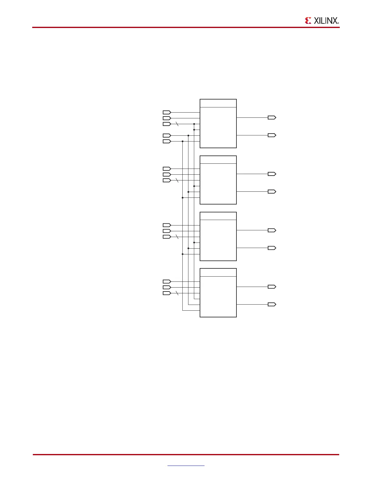
Figure 5-27 illustrates the details of distributed RAM implemented in a Virtex-5 FPGA
slice. Some elements of the slice are omitted for clarity. Only the elements relevant to the
timing paths described in this section are shown.
X-Ref Target - Figure 5-27
Figure 5-27: Simplified Virtex-5 FPGA SLICEM Distributed RAM
UG190_5_27_050506
6
D
DX
DI
D input
CX
CI
C input
BX
BI
B input
AX
AI
A input
CLK
WE
WA[6:0]
RAM
CLK
WE
DI1
DI2
A[6:0]
O6
DMUX
O5
6
C
WA[6:0]
RAM
CLK
WE
DI1
DI2
A[6:0]
O6
CMUX
O5
6
B
WA[6:0]
RAM
CLK
WE
DI1
DI2
A[6:0]
O6
BMUX
O5
6
A
WA[6:0]
RAM
CLK
WE
DI1
DI2
A[6:0]
O6
AMUX
O5
 Loading...


