Virtex-5 FPGA User Guide www.xilinx.com 91
UG190 (v5.0) June 19, 2009
Introduction
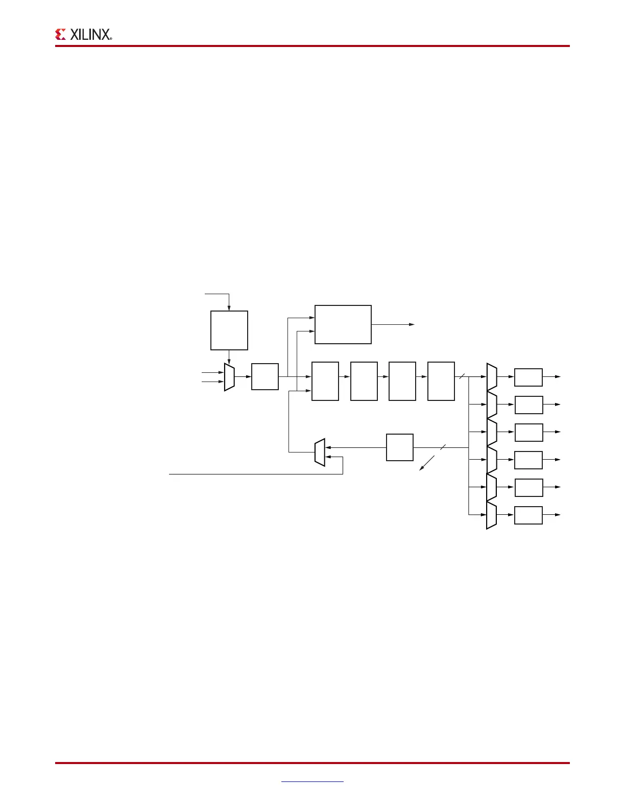
Input muxes select the reference and feedback clocks from either the IBUFG, BUFG, IBUF,
PLL outputs, or one of the DCMs. Each clock input has a programmable counter D. The
Phase-Frequency Detector (PFD) compares both phase and frequency of the input
(reference) clock and the feedback clock. Only the rising edges are considered because as
long as a minimum High/Low pulse is maintained, the duty cycle is not important. The
PFD is used to generate a signal proportional to the phase and frequency between the two
clocks. This signal drives the Charge Pump (CP) and Loop Filter (LF) to generate a
reference voltage to the VCO. The PFD produces an up or down signal to the charge pump
and loop filter to determine whether the VCO should operate at a higher or lower
frequency. When VCO operates at too high of a frequency, the PFD activates a down signal,
causing the control voltage to be reduced decreasing the VCO operating frequency. When
the VCO operates at too low of a frequency, an up signal will increase voltage. The VCO
produces eight output phases. Each output phase can be selected as the reference clock to
the output counters (Figure 3-3.) Each counter can be independently programmed for a
given customer design. A special counter, M, is also provided. This counter controls the
feedback clock of the PLL allowing a wide range of frequency synthesis.
X-Ref Target - Figure 3-3
Figure 3-3: Detailed PLL Block Diagram
D
Clock
Switch
Circuit
M
8
PFD
Lock Detect
Lock
Lock Monitor
CLKIN1
General
Routing
CLKIN2
CLKFB
CLKFBOUT
VCO feedback phase
selection for negative
phase-shift affecting
all outputs
CP LF VCO
8-phase
taps
O0
O1
O2
O3
UG190_c3_03_022709
O4
O5
 Loading...


