Virtex-5 FPGA User Guide www.xilinx.com 35
UG190 (v5.0) June 19, 2009
Global Clocking Resources
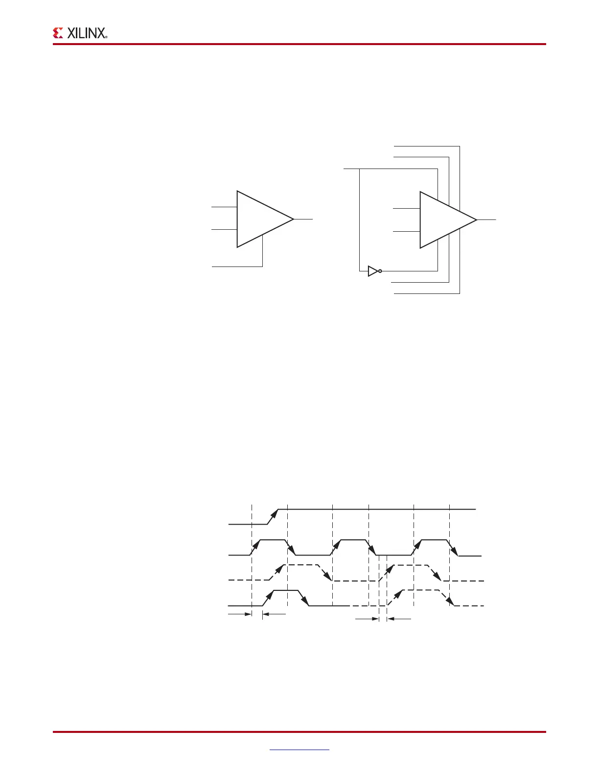
BUFGMUX_CTRL
BUFGMUX_CTRL is a clock buffer with two clock inputs, one clock output, and a select
line. This primitive is based on BUFGCTRL with some pins connected to logic High or
Low. Figure 1-11 illustrates the relationship of BUFGMUX_CTRL and BUFGCTRL.
BUFGMUX_CTRL uses the S pins as select pins. S can switch anytime without causing a
glitch. The Setup/Hold time on S is for determining whether the output will pass an extra
pulse of the previously selected clock before switching to the new clock. If S changes as
shown in Figure 1-12, prior to the setup time T
BCCCK_S
and before I0 transitions from High
to Low, then the output will not pass an extra pulse of I0. If S changes following the hold
time for S, then the output will pass an extra pulse. If S violates the Setup/Hold
requirements, the output might pass the extra pulse, but it will not glitch. In any case, the
output will change to the new clock within three clock cycles of the slower clock.
The Setup/Hold requirements for S0 and S1 are with respect to the falling clock edge
(assuming INIT_OUT = 0), not the rising edge as for CE0 and CE1.
Switching conditions for BUFGMUX_CTRL are the same as the S pin of BUFGCTRL.
Figure 1-12 illustrates the timing diagram for BUFGMUX_CTRL.
Other capabilities of the BUFGMUX_CTRL primitive are:
• Pre-selection of I0 and I1 input after configuration.
• Initial output can be selected as High or Low after configuration.
X-Ref Target - Figure 1-11
Figure 1-11: BUFGMUX_CTRL as BUFGCTRL
X-Ref Target - Figure 1-12
Figure 1-12: BUFGMUX_CTRL Timing Diagram
IGNORE1
IGNORE0
CE1
S
CE0
S1
S0
I1
I0
O
BUFGMUX_CTRL
UG190_1_11_052009
V
DD
V
DD
O
I1
I0
S
GND
GND
S
I0
I1
O
UG190_1_12_061909
T
BCCKO_O
T
BCCKO_O
 Loading...


