34 www.xilinx.com Virtex-5 FPGA User Guide
UG190 (v5.0) June 19, 2009
Chapter 1: Clock Resources
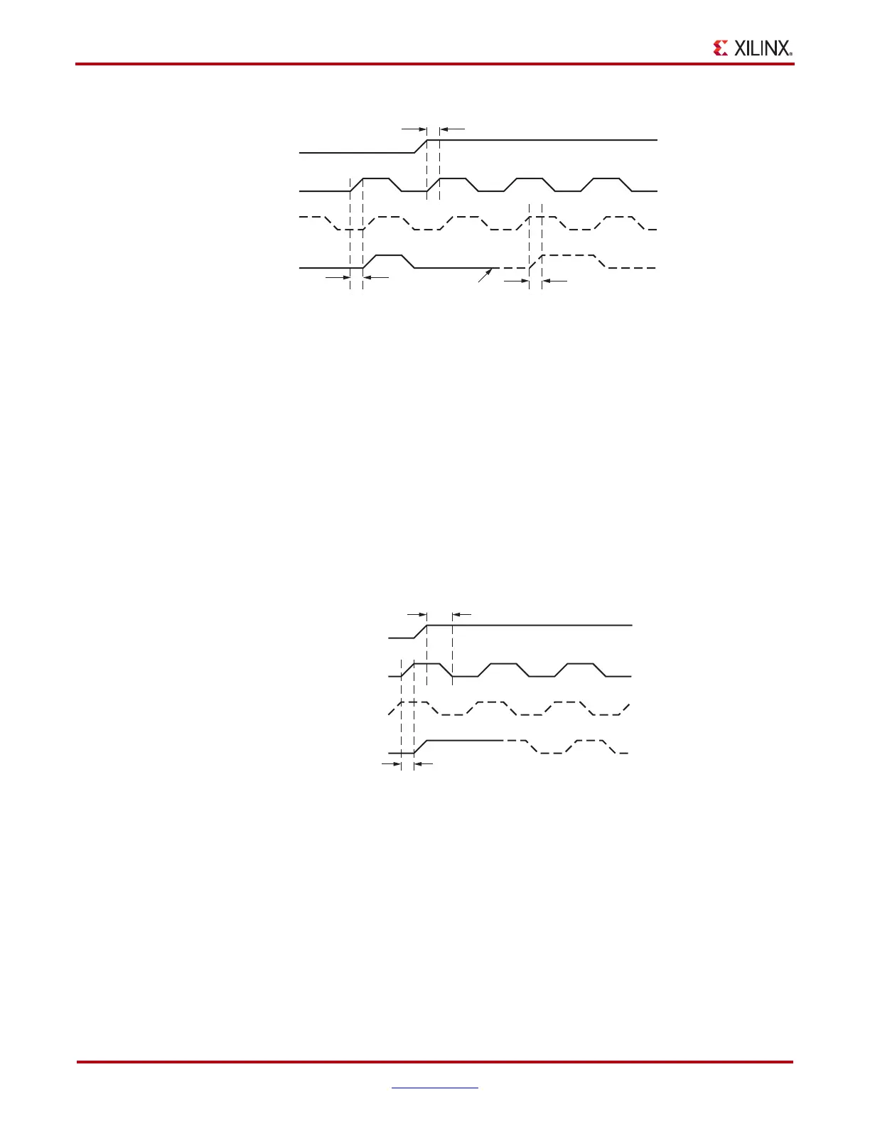
In Figure 1-9:
• The current clock is I0.
• S is activated High.
• If I0 is currently High, the multiplexer waits for I0 to deassert Low.
• Once I0 is Low, the multiplexer output stays Low until I1 transitions High to Low.
• When I1 transitions from High to Low, the output switches to I1.
• If Setup/Hold are met, no glitches or short pulses can appear on the output.
BUFGMUX_1 is rising edge sensitive and held at High prior to input switch. Figure 1-10
illustrates the timing diagram for BUFGMUX_1. A LOC constraint is available for
BUFGMUX and BUFGMUX_1.
In Figure 1-10:
• The current clock is I0.
• S is activated High.
• If I0 is currently Low, the multiplexer waits for I0 to be asserted High.
• Once I0 is High, the multiplexer output stays High until I1 transitions Low to High.
• When I1 transitions from Low to High, the output switches to I1.
• If Setup/Hold are met, no glitches or short pulses can appear on the output.
X-Ref Target - Figure 1-9
Figure 1-9: BUFGMUX Timing Diagram
X-Ref Target - Figure 1-10
Figure 1-10: BUFGMUX_1 Timing Diagram
S
I0
I1
O
T
BCCKO_O
ug190_1_09_032306
T
BCCKO_O
T
BCCCK_CE
begin
switching using I1
S
I0
I1
O
ug190_1_10_032306
TBCCCK_CE
TBCCKO_O
 Loading...


