Virtex-5 FPGA User Guide www.xilinx.com 33
UG190 (v5.0) June 19, 2009
Global Clocking Resources
Figure 1-7 illustrates the timing diagram for BUFGCE_1.
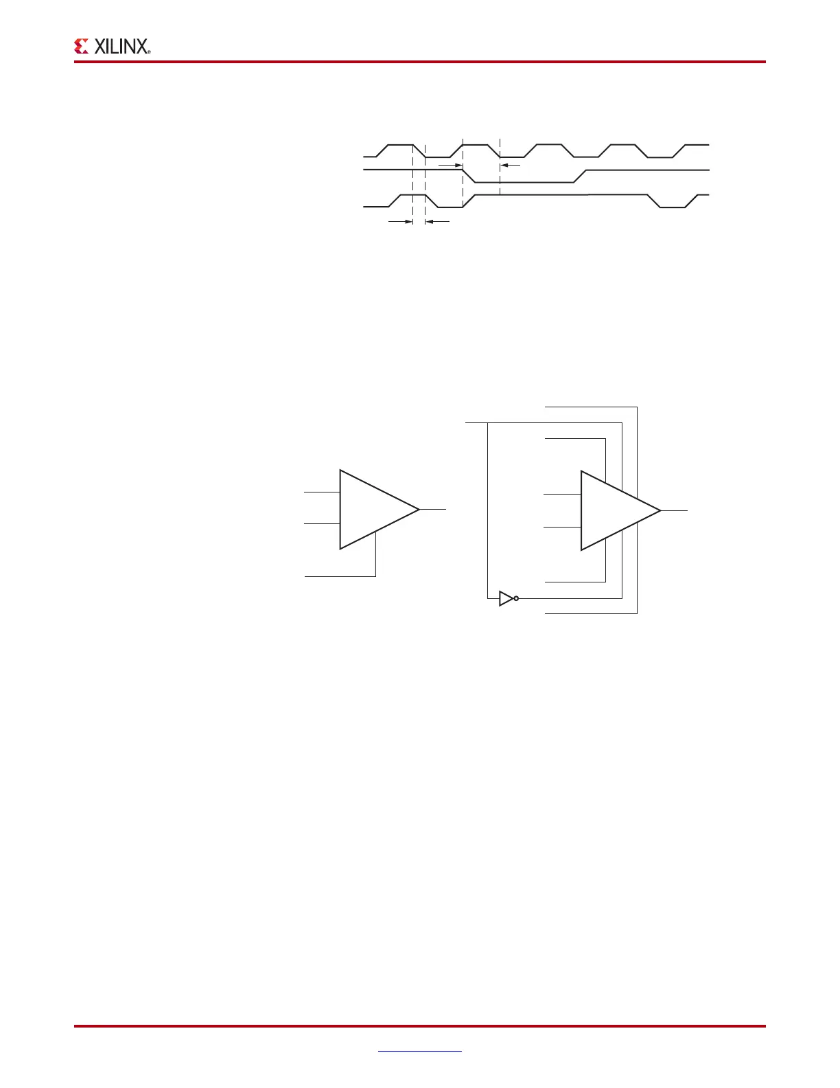
BUFGMUX and BUFGMUX_1
BUFGMUX is a clock buffer with two clock inputs, one clock output, and a select line. This
primitive is based on BUFGCTRL with some pins connected to logic High or Low.
Figure 1-8 illustrates the relationship of BUFGMUX and BUFGCTRL. A LOC constraint is
available for BUFGMUX and BUFGCTRL.
Since the BUFGMUX uses the CE pins as select pins, when using the select, the setup time
requirement must be met. Violating this setup time might result in a glitch.
Switching conditions for BUFGMUX are the same as the CE pins on BUFGCTRL.
Figure 1-9 illustrates the timing diagram for BUFGMUX.
X-Ref Target - Figure 1-7
Figure 1-7: BUFGCE_1 Timing Diagram
X-Ref Target - Figure 1-8
Figure 1-8: BUFGMUX as BUFGCTRL
BUFGCE_1(I)
BUFGCE_1(CE)
BUFGCE_1(O)
ug190_1_07_032206
T
BCCKO_O
T
BCCCK_CE
IGNORE1
IGNORE0
CE1S
CE0
S1
S0
I1
I0
O
BUFGMUX
ug190_1_08_032206
V
DD
V
DD
O
I1
I0
S
GND
GND
 Loading...


