Virtex-5 FPGA User Guide www.xilinx.com 37
UG190 (v5.0) June 19, 2009
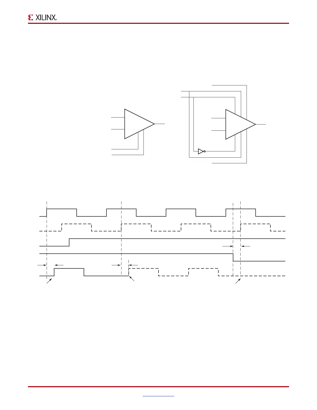
Global Clocking Resources
BUFGMUX_CTRL with a Clock Enable
A BUFGMUX_CTRL with a clock enable BUFGCTRL configuration allows the user to
choose between the incoming clock inputs. If needed, the clock enable is used to disable
the output. Figure 1-15 illustrates the BUFGCTRL usage design example and Figure 1-16
shows the timing diagram.
In Figure 1-16:
• At time event 1, output O uses input I0.
• Before time event 2, S is asserted High.
• At time T
BCCKO_O
, after time event 2, output O uses input I1. This occurs after a High
to Low transition of I0 followed by a High to Low transition of I1 is completed.
• At time T
BCCCK_CE
, before time event 3, CE is asserted Low. The clock output is
switched Low and kept at Low after a High to Low transition of I1 is completed.
X-Ref Target - Figure 1-15
Figure 1-15: BUFGMUX_CTRL with a CE and BUFGCTRL
IGNORE1
IGNORE0
CE1
S
CE
CE
CE0
S1
S0
I1
I0
O
BUFGMUX_CTRL+CE
Design Example
UG190_1_15_052009
O
I1
I0
S
GND
GND
X-Ref Target - Figure 1-16
Figure 1-16: BUFGMUX_CTRL with a CE Timing Diagram
ug190_1_16_040907
T
BCCKO_O
T
BCCCK_CE
T
BCCKO_O
at I0 Clock Off
I0
I1
S
CE
O
Begin I1
12 3
 Loading...


