278 www.xilinx.com Virtex-5 FPGA User Guide
UG190 (v5.0) June 19, 2009
Chapter 6: SelectIO Resources
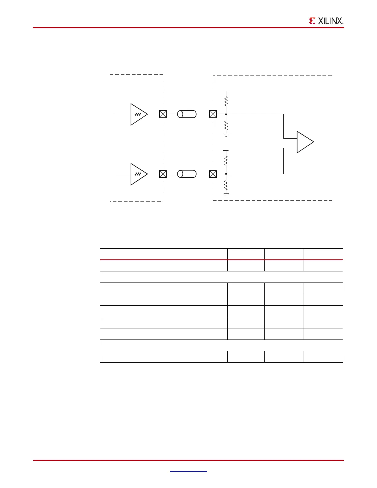
Figure 6-69 shows a sample circuit illustrating a valid termination technique for
differential SSTL2 Class I (2.5V) with unidirectional DCI termination.
Table 6-29 lists the differential SSTL2 Class I DC voltage specifications.
X-Ref Target - Figure 6-69
Figure 6-69: Differential SSTL2 (2.5V) Class I Unidirectional DCI Termination
Table 6-29: Differential SSTL2 Class I DC Voltage Specifications
Min Typ Max
V
CCO
2.3 2.5 2.7
Input Parameters
V
TT
–V
CCO
× 0.5 –
V
IN
(DC)
(1)
–0.30 – V
CCO
+0.30
V
ID
(DC)
(2)
0.3 – V
CCO
+0.60
V
ID
(AC) 0.62 – V
CCO
+0.60
V
IX
(AC)
(3)
0.95 – 1.55
Output Parameters
V
OX
(AC)
(4)
1.0 – 1.5
Notes:
1. V
IN
(DC) specifies the allowable DC excursion of each differential input.
2. V
ID
(DC) specifies the input differential voltage required for switching.
3. V
IX
(AC) indicates the voltage where the differential input signals must cross.
4. V
OX
(AC) indicates the voltage where the differential output signals must cross.
ug190_6_65_030506
IOB
DIFF_SSTL2_I_DCI
DIFF_SSTL2_I_DCI
V
CCO
= 2.5V
2R
VRP
= 2Z
0
= 100Ω
2R
VRN
= 2Z
0
= 100Ω
+
–
DCI
DIFF_SSTL2_I_DCI
V
CCO
= 2.5V
2R
VRP
= 2Z
0
= 100Ω
2R
VRN
= 2Z
0
= 100Ω
Z
0
Z
0
R
0
= 25Ω
R
0
= 25Ω
 Loading...


