222 www.xilinx.com Virtex-5 FPGA User Guide
UG190 (v5.0) June 19, 2009
Chapter 6: SelectIO Resources
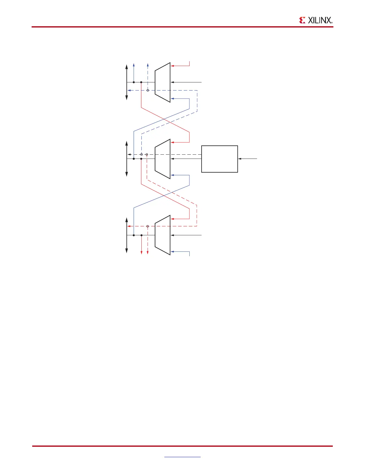
The guidelines when using DCI cascading are as follows:
• The master and slave banks must all reside on the same column (left, center, or right)
on the device.
• Master and slave banks must have the same V
CCO
and V
REF
(if applicable) voltage.
• DCI I/O banking compatibility rules must be satisfied across all master and slave
banks (for example, only one DCI I/O standard using single termination type is
allowed across all master and slave banks). DCI I/O standard compatibility is not
constrained to one bank when DCI cascading is implemented; it extends across all
master and slave banks.
X-Ref Target - Figure 6-5
Figure 6-5: DCI Cascading Supported Over Multiple Banks
UG190_6_96_012907
DCI VRN/VRP
Bank A
Bank B
Bank C
To
Local
Bank
To
Local
Bank
To
Local
Bank
To Banks Above
(When Cascaded)
To Banks Below
(When Cascaded)
 Loading...


