324 www.xilinx.com Virtex-5 FPGA User Guide
UG190 (v5.0) June 19, 2009
Chapter 7: SelectIO Logic Resources
Note: The DDLY timing diagrams and parameters are identical to the D timing diagrams and
parameters.
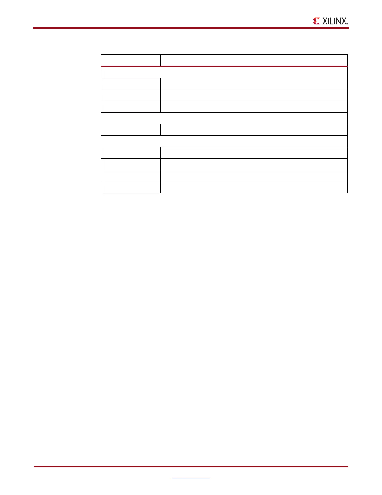
Table 7-5: ILOGIC Switching Characteristics
Symbol Description
Setup/Hold
T
ICE1CK
/T
ICKCE1
CE1 pin Setup/Hold with respect to CLK
T
ISRCK
/T
ICKSR
SR/REV pin Setup/Hold with respect to CLK
T
IDOCK
/T
IOCKD
D pin Setup/Hold with respect to CLK
Combinatorial
T
IDI
D pin to O pin propagation delay, no Delay
Sequential Delays
T
IDLO
D pin to Q1 pin using flip-flop as a latch without Delay
T
ICKQ
CLK to Q outputs
T
ICE1Q
CE1 pin to Q1 using flip-flop as a latch, propagation delay
T
RQ
SR/REV pin to OQ/TQ out
 Loading...


