194 www.xilinx.com Virtex-5 FPGA User Guide
UG190 (v5.0) June 19, 2009
Chapter 5: Configurable Logic Blocks (CLBs)
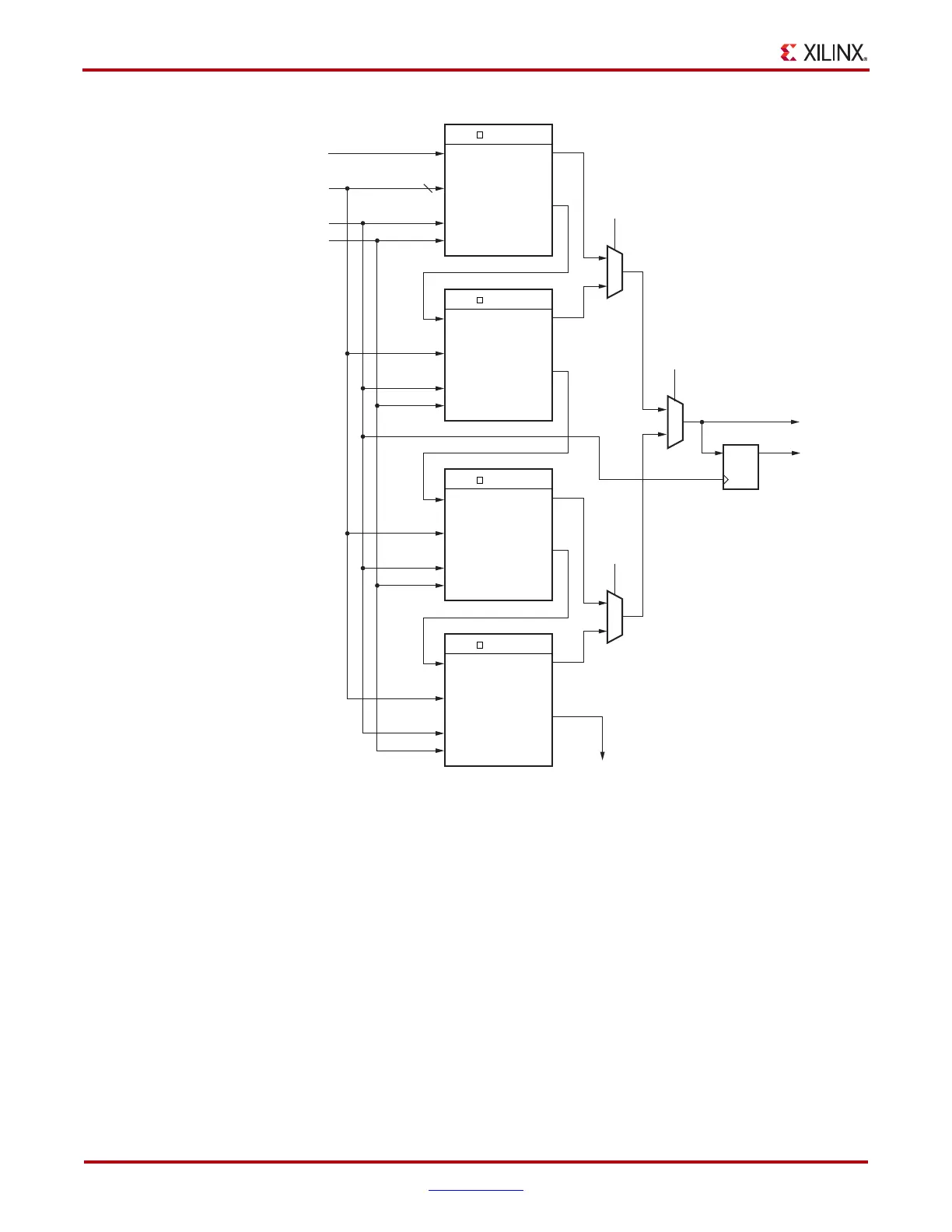
It is possible to create shift registers longer than 128 bits across more than one SLICEM.
However, there are no direct connections between slices to form these shift registers.
Shift Register Data Flow
Shift Operation
The shift operation is a single clock-edge operation, with an active-High clock enable
feature. When enable is High, the input (D) is loaded into the first bit of the shift register.
Each bit is also shifted to the next highest bit position. In a cascadable shift register
configuration, the last bit is shifted out on the M31 output.
The bit selected by the 5-bit address port (A[4:0]) appears on the Q output.
Dynamic Read Operation
The Q output is determined by the 5-bit address. Each time a new address is applied to the
5-input address pins, the new bit position value is available on the Q output after the time
X-Ref Target - Figure 5-20
Figure 5-20: 128-bit Shift Register Configuration
UG190_5_20_050506
DI1
SHIFTIN (D)
A[6:0]
CLK
WE
(CLK)
(WE/CE)
5
SRL32
A[6:2]
CLK
WE
O6
MC31
MC31
MC31
MC31
DI1
SRL32
A[6:2]
CLK
WE
O6
F7BMUX
F8MUX
CX (A5)
BX (A6)
Registered
Output
Output (Q)
(Optional)
DQ
(BMUX)
SHIFTOUT (Q127)
(MC31)
(BQ)
DI1
SRL32
A[6:2]
CLK
WE
O6
DI1
SRL32
A[6:2]
CLK
WE
O6
F7AMUX
AX (A5)
 Loading...


