232 www.xilinx.com Virtex-5 FPGA User Guide
UG190 (v5.0) June 19, 2009
Chapter 6: SelectIO Resources
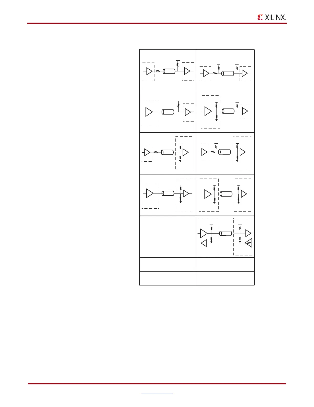
X-Ref Target - Figure 6-17
Figure 6-17: SSTL DCI Usage Examples
ug190_6_15_041106
Conventional
DCI Transmit
Conventional
Receive
Conventional
Transmit
DCI Receive
DCI Transmit
DCI Receive
Bidirectional
Reference
Resistor
Recommended
Z
0
(2)
VRN = VRP = R = Z
0
50 Ω
VRN = VRP = R = Z
0
50 Ω
SSTL2_I or SSTL18_I SSTL2_II or SSTL18_II
N/A
Z
0
R
V
CCO
/2
Z
0
R/2
RR
V
CCO
/2 V
CCO
/2
Z
0
R/2
R
V
CCO/2
Z
0
R/2
2R
2R
V
CCO
Z
0
R/2
2R
2R
V
CCO
2R
R
V
CCO
V
CCO
/2
2R
Z
0
R
V
CCO
/2
Z
0
2R
2R
V
CCO
2R
2R
V
CCO
Z
0
2R
2R
V
CCO
Z
0
2R
2R
V
CCO
2R
2R
V
CCO
25Ω
(1)
25Ω
(1)
25Ω
(1)
25Ω
(1)
25Ω
(1)
25Ω
Virtex-5
DCI
Virtex-5
DCI
Virtex-5
DCI
Virtex-5
DCI
Virtex-5 DCI
Virtex-5
DCI
Virtex-5
DCI
Virtex-5
DCI
Virtex-5
DCI
Virtex-5
DCI
Notes:
1. The SSTL-compatible 25 Ω or 20 Ω series resistor is accounted for in the DCI buffer,
and it is not DCI controlled.
2. Z
0
is the recommended PCB trace impedance.
 Loading...


