Virtex-5 FPGA User Guide www.xilinx.com 287
UG190 (v5.0) June 19, 2009
Specific Guidelines for I/O Supported Standards
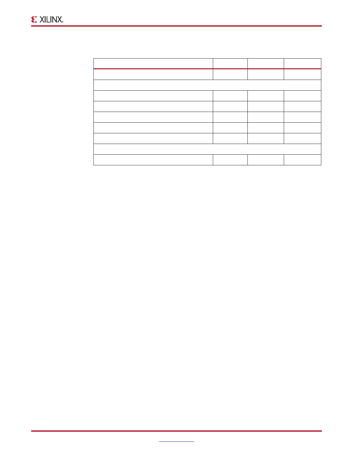
Table 6-32 lists the differential SSTL (1.8V) Class I DC voltage specifications.
Table 6-32: Differential SSTL (1.8V) Class I and Class II DC Voltage Specifications
Min Typ Max
V
CCO
1.7 1.8 1.9
Input Parameters
V
TT
–V
CCO
× 0.5 –
V
IN
(DC)
(1)
–0.30 – V
CCO
+0.30
V
ID
(DC)
(3)
0.25 – V
CCO
+0.60
V
ID
(AC) 0.50 – V
CCO
+0.60
V
IX
(AC)
(4)
0.675 – 1.125
Output Parameters
V
OX
(AC)
(5)
0.725 – 1.075
Notes:
1. V
IN
(DC) specifies the allowable DC excursion of each differential input.
2. Per EIA/JESD8-6, “The value of V
REF
is to be selected by the user to provide optimum noise margin in
the use conditions specified by the user.”
3. V
ID
(DC) specifies the input differential voltage required for switching.
4. V
IX
(AC) indicates the voltage where the differential input signals must cross.
5. V
OX
(AC) indicates the voltage where the differential output signals must cross.
 Loading...


