290 www.xilinx.com Virtex-5 FPGA User Guide
UG190 (v5.0) June 19, 2009
Chapter 6: SelectIO Resources
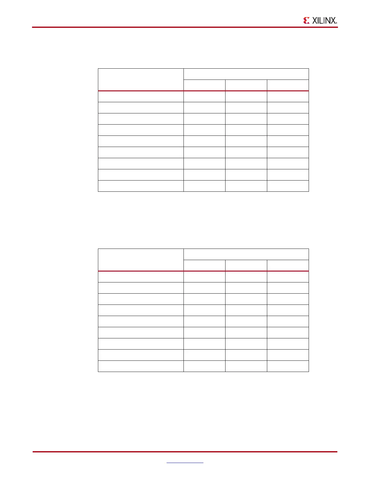
Table 6-33 and Table 6-34 lists the SSTL (1.8V) DC voltage specifications for Class I and
Class II, respectively.
Table 6-33: SSTL (1.8V) DC Voltage Specifications Class I
Class I
Min Typ Max
V
CCO
1.7 1.8 1.9
V
REF
=0.5× V
CCO
0.833 0.9 0.969
V
TT
=V
REF
+N
(1)
0.793 0.9 1.009
V
IH
≥ V
REF
+ 0.125 0.958 – V
CCO
+0.3
(2)
V
IL
≤ V
REF
– 0.125 –0.3
(3)
–0.844
V
OH
≥ V
TT
+0.47
(4)
1.263 – –
V
OL
≤ V
TT
–0.47
(4)
– – 0.539
I
OH
at V
OH
(mA) –6.7 – –
I
OL
at V
OL
(mA) 6.7 – –
Notes:
1. N must be greater than or equal to –0.04 and less than or equal to 0.04.
2. V
IH
maximum is V
CCO
+0.3.
3. V
IL
minimum does not conform to the formula.
4. Because SSTL_I_DCI uses a controlled-impedance driver, V
OH
and V
OL
are different.
Table 6-34: SSTL (1.8V) DC Voltage Specifications Class II
Class II
Min Typ Max
V
CCO
1.7 1.8 1.9
V
REF
=0.5× V
CCO
0.833 0.9 0.969
V
TT
=V
REF
+N
(1)
0.793 0.9 1.009
V
IH
≥ V
REF
+ 0.125 0.958 – V
CCO
+0.3
(2)
V
IL
≤ V
REF
– 0.125 –0.3
(3)
–0.844
V
OH
≥ V
TT
+ 0.603
(4)
1.396 – –
V
OL
≤ V
TT
–0.603
(4)
– – 0.406
I
OH
at V
OH
(mA) –13.4 – –
I
OL
at V
OL
(mA) 13.4 – –
Notes:
1. N must be greater than or equal to –0.04 and less than or equal to 0.04.
2. V
IH
maximum is V
CCO
+0.3.
3. V
IL
minimum does not conform to the formula.
4. Because SSTL_I_DCI uses a controlled-impedance driver, V
OH
and V
OL
are different.
 Loading...


